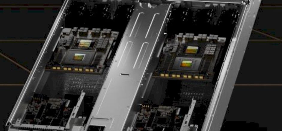
Updated With More MGX Specs: Whenever a compute engine maker also does motherboards as well as system designs, those companies that make motherboards (there are dozens who do) and create system designs (the original design manufacturers and the original – get a little bit nervous as well as a bit relieved. The standardization of components means there is less for them to do, but at the same time, there is less for them to charge for.
With its MGX multi-generational server platform designs, announced this week at the Computex trade show in Taiwan, which is one of the major centers in the world for component and system manufacturing as well as the undisputed center of compute engine manufacturing and assembly, Nvidia is hoping to make life easier for itself and the OEMs and ODMs of the world and provide better profits for itself and for them.
Nvidia has been making its own servers since the DGX-1 system debuted in April 2016 based on the “Pascal” P100 GPU accelerator. Nvidia decided to do this go help speed up time to market and to create a feedback loop into component and motherboard designs; the fact that Nvidia needed to build its own supercomputers to run its massive AI workloads – which was cheaper than having an OEM or ODM do it – was also a contributing factor in the decision. At the time, most of the Pascal GPUs that Nvidia could have manufactured were shipping to the hyperscalers and cloud builders as well as a few HPC centers, and the DGX-1s were being sold by Nvidia in a preferential manner so researchers and scientists could get their hands on these GPU-accelerated systems. This was still the case in May 2017 when the DGX-1 machines were updated with the “Volta” V100 GPU accelerators announced two months earlier. The DGX-A100 system followed in May 2020, using the “Ampere” A100 GPUs, and of course the DGX-H100 design, which scales out a lot further with an NVLink Switch fabric, rolled out concurrently with the “Hopper” H100 GPU accelerator last year and was just updated this week with a hybrid CPU-GPU design in the DGX-GH200 system.
You can’t buy an H100 SXM5 or NVSwitch 3 ASIC used in the latest DGX-H100 and DGX-GH200 machines. The system boards for CPUs, GPUs, and NVSwitch interconnects are sold to hyperscalers and cloud builders and their ODM suppliers as a unit, with all of the components manufactured and tested, and are also sold to OEMs as preassembled components, which they in turn put into their systems. You can buy PCI-Express versions of the GPU accelerators or Quantum InfiniBand or Spectrum Ethernet ASICs from Nvidia if you want to build your own systems, but for the high-end stuff running on a the NVSwitch memory fabric, you have to take these preassembled components, which are called HGX.
Having standardized the inside components of the systems to a certain extent with HGX/DGX, Nvidia now wants to standardize the shells that wrap around these components to speed up the time to market for all ODMs and OEMs and to make it so the resulting systems can be upgraded in the field to the largest extent possible given whatever future architectural changes will be coming down the pike.
That, in a nutshell, is what the MGX effort is all about.
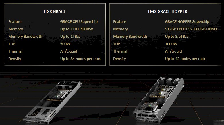
We got a little taste of what the initial MGX designs look like last May when the prototype HGX Grace and HGX Grace-Hopper system designs were divulged by Nvidia. These were not just system boards, but complete rack-mounted server designs:
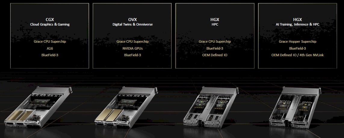
The MGX standardization effort will span the DGX/HGX datacenter compute platforms, the OVX metaverse hosting platforms, and CGX cloud graphics and gaming platforms, and here is how Nvidia said the Grace CPU and various GPU accelerators would be composed for these three lines of iron:
Here are the MGX designs that it was showing off at Computex this week:
The one on the left is a Grace-Grace superchip paired with four GPU accelerators. The system in the center has two X86 CPUs, two ConnectX network interfaces, and eight GPU accelerators, and the system on the right has a pair of water-cooled compute engines (we are guessing Grace-Hopper superchips) and two network interface cards.
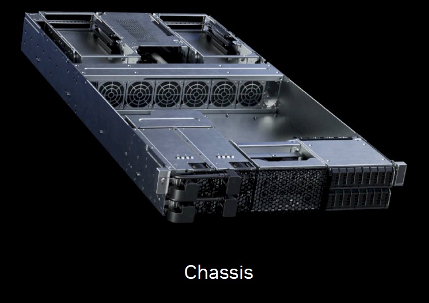
The company’s Web site and prebriefings did not explain these as well as Nvidia co-founder and chief executive officer, Jensen Huang, did in his keynote, when he walked through some of the aspects of the MGX system, starting with the 2U chassis:
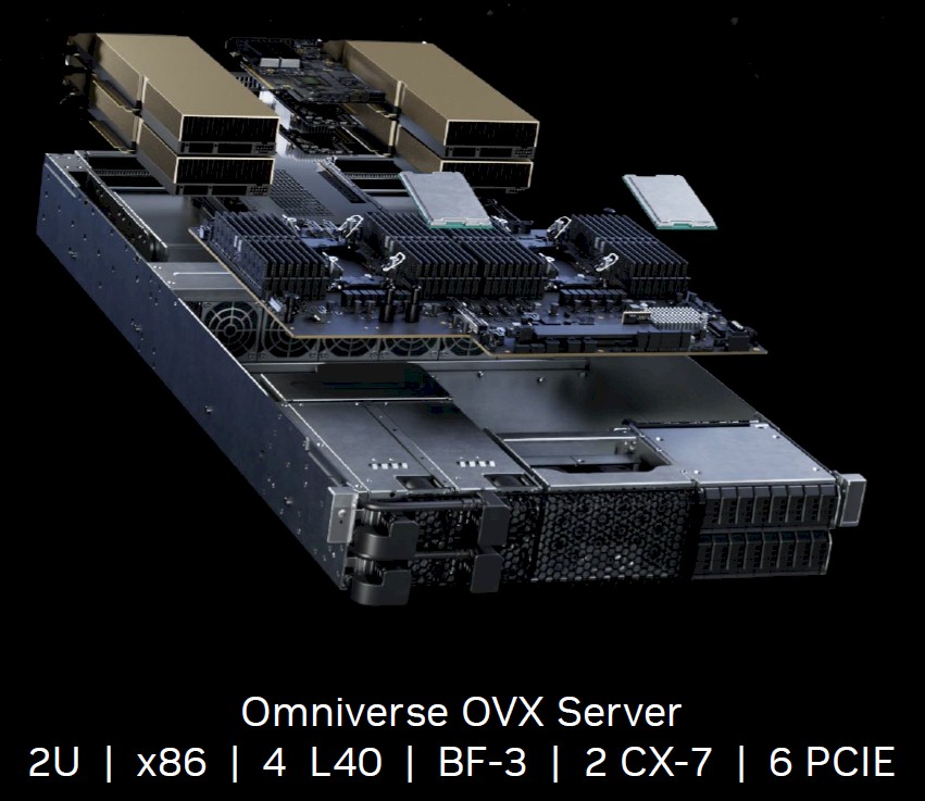
When you add two X86 CPUs, four L40 GPU accelerators, a BlueField-3 DPU, a pair of ConnectX-7 network interface cards, and leave open six PCI-Express 5.0 slots, you get an OVX server for accelerating Nvidia’s Omniverse virtual reality digital twin software stack:
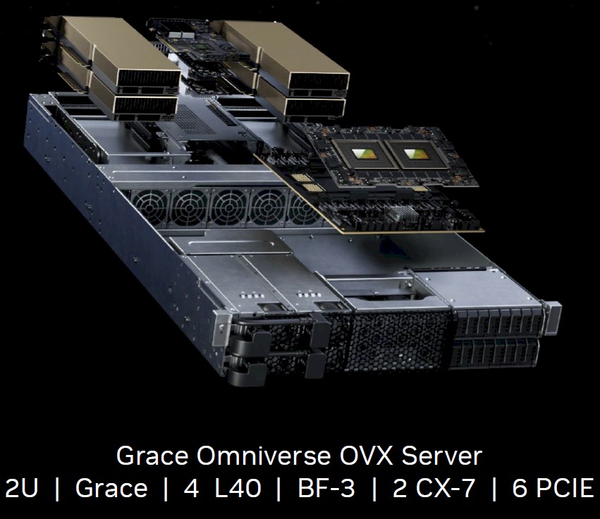
You can pop out the pair of X86 CPUs and put in one Grace-Grace superchip and all the same stuff (with one fewer PCI-Express 5.0 slot) and you get this variant of the OVX server:
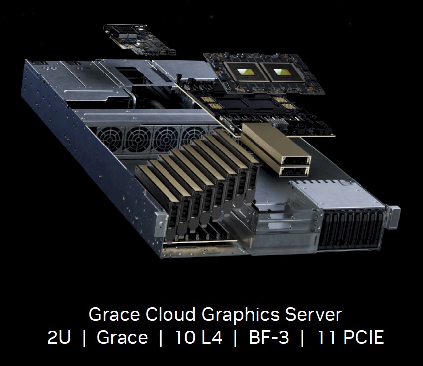
If you want to do cloud graphics for rendering or gaming or modest AI inference workloads, what Nvidia calls a CGX machine, you can start with the MGX chassis and put in a Grace-Grace superchip, ten L4 GPU accelerators, a BlueField-3 DPU and have 11 PCI-Express 5.0 slots open and it looks like this:
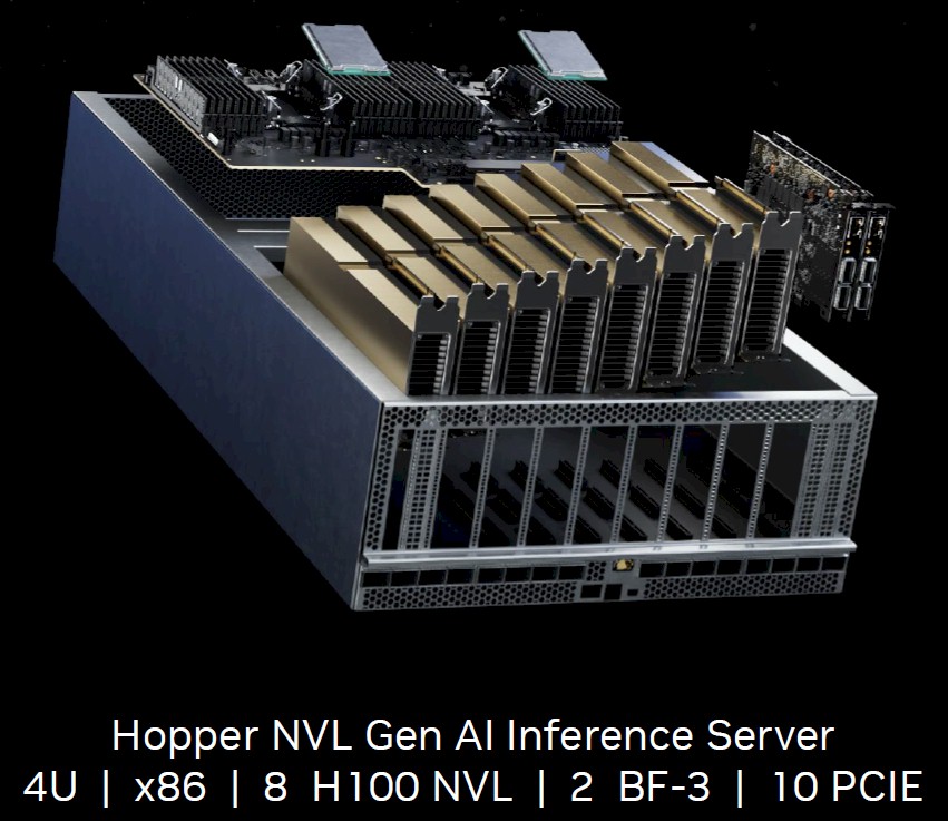
If you need to drive denser AI inference workloads, particularly for LLMs and DLRMs, then you grab the 4U version of the MGX chassis, you pop in a pair of X86 CPUs, eight of the double-wide H100 NVL accelerators, a pair of BlueField-3 DPUs and have ten PCI-Express slots left and you get this:
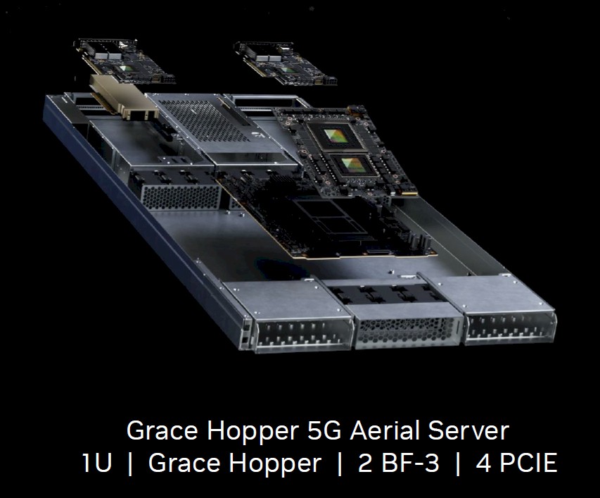
For 5G use cases, think thinner and smaller, just like NEBS-compliant telco machines have been for decades. Here is what the Grace-Hopper 5G arial server design looks like:
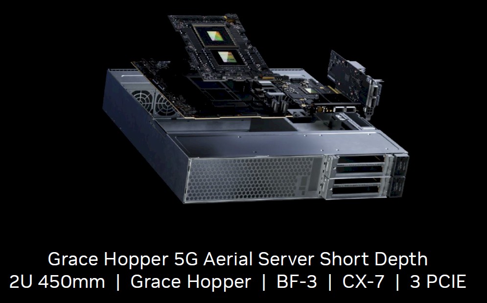
This is a 1U MGX pizza box chassis with a single Grace-Grace superchip, a pair of the BlueField-3 DPUs, with four open PCI-Express 5.0 slots for peripherals. And for tight point of presence (POP) spaces at telcos and other service providers, you have to double up the height and half the length of the chassis like this:
For whatever reason, one of the PCI-Express slots is configured with a ConnectX-7 NIC as well as a single BlueField-3 DPU. (The form factor should not affect the networking, so we presume Nvidia was just showing options.)
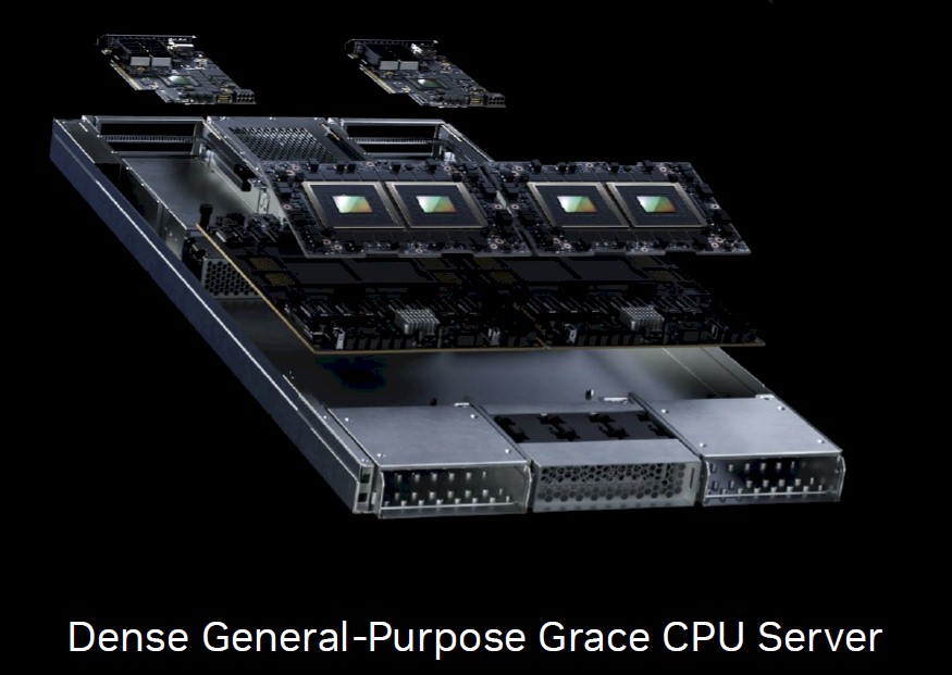
If you were wondering, as we were, what the “whitebox” server nodes in the “Isambard 3” supercomputer going into the GW4 collective in the United Kingdom later this year might look like, now we know:
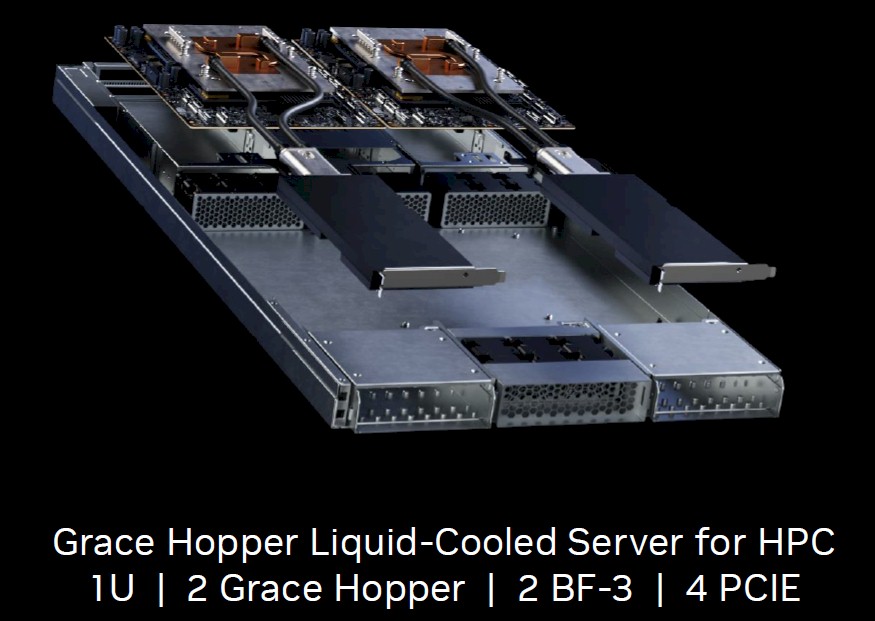
And for very dense HPC machines that can’t rely on air-cooling (or liquid cooling in the racks like Isambard 3 does), there is a liquid-cooled variant of the MGX with a pair of Grace-Grace superchips:
Howdy, Pardner!
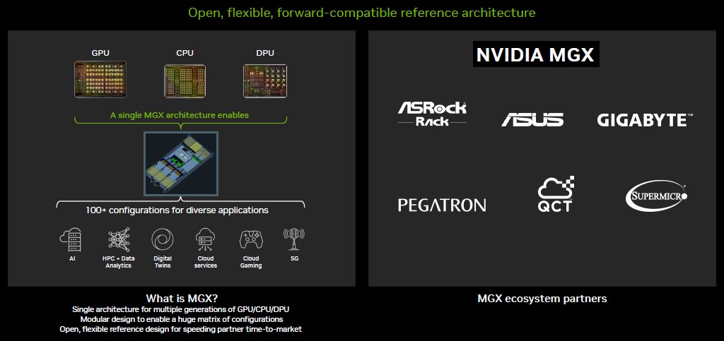
Nvidia is starting out with eight key MGX partners, many of whom are motherboard makers and ODM system manufacturers. These include ASRock, ASUS, Gigabyte, Pegatron, Quanta Cloud Technology, and Supermicro. The idea is to provide over one hundred different server designs that can be targeted to a wide array of workloads, spanning AI, HPC, data analytics, digital twins, cloud infrastructure, cloud gaming, and 5G networking.
The MGX reference architectures will include systems with 1U, 2U, and 4U rack enclosures that are available with both air and liquid cooling. The idea is to support the full Nvidia GPU accelerator portfolio, starting with the Hopper H100 compute engines and the “Lovelace” L4 and L40 AI inference and graphics accelerators. On the CPU front, the Grace-Grace superchip (it has not been given a name but GG200 makes sense) and the Grace-Hopper superchip (called the GH200) are central, but X86 processors, presumably from both Intel and AMD, will be included in the MGX designs. (By the way, as far as we can tell, you can’t have just one Grace CPU, which we would call a CG100 if we had to name the chip and a C100 as its marketing name if we were going to be consistent with how Nvidia names its datacenter compute engines this far.) As for networking, the MGX specs start with the ConnectX-7 hybrid InfiniBand/Ethernet network interface cards and the BlueField-3 DPUs.
As far as we know, MGX designs will not be backcast to prior GPUs, CPUs, DPUs, or NICs. This is a very forward looking thing.
Supermicro’s ARS-221GL-NR system, which was unveiled at Computex, will include the Grace-Grace superchip in an existing MGX design and QCT’s S74G-2U system is using an MGX design with the Grace-Hopper superchip. SoftBank, the owner of Arm Holdings, plans to use MGX designs in multiple hyperscale datacenters in Japan and dynamically allocate GPU processing capacity across 5G and generative AI applications its conglomerate companies run.
When we talked to Charlie Boyle, vice president of the DGX line at Nvidia and also the executive who is spearheading the MGX effort, we suggested that MGX was a bit like the Cray “Cascade” and “Shasta” server designs in that they allowed for multiple generations of compute and interconnects to be housed in them, allowing Cray to spread the cost of system designs out over different kinds of compute and networking and across more than one generation, too. He laughed.
“I don’t know that I would make the comparison to Cray,” Boyle said. “I’ve been in this industry a long time to, you know, and it’s very bespoke system.”
OK, that’s fair enough, but it wasn’t the point. A comparison to Facebook’s Open Compute Project was a little more palatable. But this is all about speed, not making metaphors.
“We are talking about the actual physical attributes inside of the system,” Boyle tells The Next Platform. “When we started out years ago with the HGX baseboard, we wanted to make it easy for our partners to get quick time to market. And for everyone that wants to build Grace-Hopper and Grace-Grace systems, and have a multi-generational guarantee on architecture, with MGX they can quickly build systems. You and I both know that Nvidia puts out new generations of technology faster than most in the market. And so the more that we can simplify designs and increase our downstream partners’ ability to ingest that technology, and then get that out to end customers more quickly, it’s great for the partners and it’s great for us.”
Boyle says that it can take 18 months to 24 months for a typical system design – costing several millions of dollars – to be constructed, tested, and qualified for manufacturing, and with MGX Nvidia can take that down to a couple of months because in the end, what ODM and OEM partners will be doing will be selecting from a menu of components and having them certified to plug together and just work. The ODM and OEM adds whatever customizations, such as BMCs and firmware updates and so on, and doing the final qualification on the assembled components.
But speed is more than that. It is about avoiding mistakes.
“In the years that I have been doing DGX, even though we build our own system, I share everything that we do with our OEM and ODM partners to help them get time to market, to show them what works and what doesn’t work, and what parts we use – all of that stuff,” says Boyle. “They are super appreciative of it because anything that we’ve already done the work on – we’ve tried, we failed, we’ve got a better component for it, whatever –if we tell them that, then they don’t need to run those same experiments, they don’t need to replicate the cost that we went through all those times over. And they are super happy about it because they are all dealing with the same thing: labor shortages and component shortages. So the fact that we do it for them, and that allows them to innovate where they can truly innovate. It’s on their overall software stack and on their overall offering. It’s about their solutions. The fact that the screws go in a different place in ten different system manufacturers designs, does that add any value to an end customer?”
This means the ODMs and OEMs will have lower R&D costs, and it also means that Nvidia can guarantee a degree of consistency out there for how its compute and networking devices are integrated into systems.
We expect that the ODMs and OEMs will think that they have special knowledge and skills and that they will resist this a bit at first. The Open Compute Project was born in conjunction with Dell, which was Facebook’s server maker for many years, because the social network wanted to move faster and remove cost. And after all this time, Dell still thinks its own hyperscale designs are better than those of either Meta Platforms or Microsoft in the Open Compute Project. Moreover, the big OEMs will be worried that the playing field will be leveled for a whole slew of smaller system makers, which will make their lives harder in a sense.
We think these smaller system makers will be more enthusiastic initially about MGX than the big OEMs like Dell, Hewlett Packard Enterprise, Lenovo, Cisco Systems, and Lenovo. But if what Boyle contends is true – that they will make more money selling MGX systems than building their own DGX clones – then they will go for it.
One last thing: It might help if the MGX designs were opened up through the Open Compute Project. Why not?




I’ll need impressed if MGX allows one to swap modules between Dell, HPE, Supermicro and Asus systems. Otherwise, not so much.
The statement “and that allows them to innovate where they can truly innovate. It’s on their overall software stack and on their overall offering.” When building a HPC or AI cluster do people really choose between Dell or HPE based on the software stack?
To use a technical term, “Hell No.” They get to differentiate on customer account and tech support for, er, Level 1 and Level 2 that passes back to Nvidia Level 3. It is perplexing a bit.
Oh yeah, what could possibly go wrong? One historically altruistic and open company driving a vertically integrated stack – rack, really. Vendors still able to contribute a badge or grille. No, I’m being totally unfair: they still also have the responsibility to choose the PSU and rail design…
Remember the olden days when “standard” was understood to mean non-proprietary and multi-source?
I do remember. I also remember 25 different system makers and maybe 40 different operating systems…. And a whole lot more profits for everyone.