

There has always been a certain amount of fear, uncertainty, and doubt that IT vendors sow as they try to protect their positions in markets that they participate in. But there is also a lot of straight-up misunderstanding among those vendors as well as the people who work at the companies that acquire IT hardware, software, and services.
And thus, these persistent myths need to be debunked from time to time. And it doesn’t take explosives to do the debunking, although we admit that would make it fun. We will leave that to special effects experts Adam Savage and Jamie Hyneman, who hosted the canonical MythBusters show from 2003 through 2017 and who debunked 1,050 myths in 248 episodes with 900 explosions.
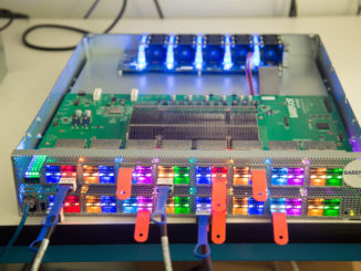
The Next Platform sat down with Lynn Comp, vice president in AMD’s server business unit, to talk about datacenter compute myths and debunk them. Here are the first five:
- Myth 1: Epyc processors from AMD can’t run all X86 workloads.
- Myth 2: Thermal design point, or TDP, is the be-all, end-all of measuring power for comparing CPUs.
- Myth 3: The ARM architecture is the best way to get low power and energy efficient compute.
- Myth 4: You have to choose between performance and efficiency – you can’t have both.
- Myth 5: Simultaneous Multi-Threading, or SMT, is “legacy X86 baggage” left over from the days before multi-core CPUs. The benefits of SMT are not worth it given the security risks or the unpredictable per core performance inherent in sharing threads on a core.
You undoubtedly have your own opinions, so don’t be shy about commenting after watching the conversation.
This content was sponsored by AMD.

Gordian Knot: Broadcom And TSMC To Cut Intel Into Two?
People are impatient for Intel to get fixed, and have been for many years. Weird deal after weird deal keeps coming out of the rumor mill, and now we have rumors that rival chip designer and seller Broadcom and rival chip manufacturer Taiwan Semiconductor Manufacturing Co want to cleave Intel …
Programming The Network With Intel NEX Chief Nick McKeown
It would be very difficult indeed to find a better general manager for Intel’s newly constituted Network and Edge Group networking business than Nick McKeown, and Pat Gelsinger, the chief executive officer charged with turning around Intel’s foundries and its chip design business, is lucky that Intel was on an …
SQUIP Side Channel Attack Rattles AMD’s Zen Cores
The majority of AMD’s CPU lineup – essentially any processor using Zen 1, Zen 2, or Zen 3 cores with simultaneous multithreading (SMT) enabled – is vulnerable to a newly disclosed side channel attack. The Scheduler Queue Usage via Interface Probing attack, or SQUIP for short, was detailed in a …
My question: what software uses the SIMD instructions (SSE/AVX) but could on the GPU? would it run better on a GPU? If so, I would be interested in a return to smaller cores w/o SIMD or perhaps a much simpler SIMD? and have more cores?
SMT was a good avenue to utilize dead cycles waiting for memory access, whether single or multi-core. But if it is a security risk, then we can give it up. Of course, if there is way control how the logical processors of a core are accessed, then we can keep it.
While a fan of big SRAM, I am not convinced super large cache is the way to use it. We should bite the bullet in embracing OS and application capable of using multi-tier memory. My preference is to have low latency memory + conventional DRAM, but if other people are thinking conventional main memory DRAM + CXL memory, then multi-tier memory is still needed
I have been saying this for years. If you really believe in accelerated computing, then why is it in the CPU? The answer is because not everyone believes in offload models.
I see your points (you could both be right), but I remember a time when the FPU was a separate chip (eg. 8087, 80287), the MMU was also a separate IC (AMD fixed that before Intel), and, these days, separate northbridges are also disappearing in favor of in-package I/O dies. Contemporary FPUs and MMUs in particular are programmable through the CPU’s ISA, as are current vector units, and one may hope (maybe) that future GPUs get similarly tightly integrated with CPUs, and into a unified instruction-space (no more need to separately feed the external data-hungry beast).
Then again, if the data processing pipeline through the GPU is too distinct from that of the CPU (eg. uncommonly systolic) these offsprings may need to be kept separated (each calling the other to “come out and play” on an as needed basis).
Maybe we literally need lego blocks of compute all linked by fast interconnects and we literally build a system for a particular workflow by connecting stuff. No more static configurations at all. I mean, imagine how much fun would it be to breadboard such a machine? Literally snapping things together and then pouring data in one end and getting answers at the other end. When the task is done, reconfigure and do a different workflow.
Maybe making FPGAs better and cheaper and faster and making electricity way, way cheaper is the real answer. I keep coming to this conclusion. That general purpose compute is actually an illusion unless it is completely reconfigurable.
A hardware system (pool of heterogeneous units) that reconfigures itself (connection-wise) dynamically to match an executing program’s computational graph (code) and data access patterns?
A most serene interview, a pastel of meditative and jovial undertones! I’m happy to hear from AMD, since the competition (Nvidia and Intel) have put out many annoucements of late, without much riposte, making me worry that the swash-buckling old-spice stronger swagger El Capitan might have run out of rhumba, or worse! I guess that this mightiest of HPC pugilists is just quietly prepping for the biggest smackdown in Exaflopping ballroom showdown history, with quiet discipline, incense, herb tea, a bit of yoga, and physics!
Mythwise (to this TNP reader) there isn’t much controversy in the 5 that were discussed. For example, we’ve seen how Frontier moved the Pareto curve for both performance and efficiency (simultaneously), and expect no less from MI300A and its siblings. SMT has its advantages in the datacenter and could be pushed to 4 or 8 threads on some SKUs, as suggested by the interviewer. The competition from ARM is interesting, and it seems to me that AMD could easily CSS-copy-paste itself some Neoverses unto MI300N and MI300V APUs for those customers that want this option, or even just for fun!
Interesting interview! I’d like to bring up an additional myth, and a question, that have been discussed in recent TNP pieces and comments, and that cloud CVP Comp may find interesting too (and maybe provide perspectives on):
Myth 6: Datacenters and factories are best located in Austin, TX, as compared to Asheville, NC.
Question: How do you view (at present and in the future) cloud-based vs on-premise HPC (eg. in light of DOE and SC23)?
I want to ask question too: is it good if AMD complete datacenter set with switch discussed here: https://www.nextplatform.com/2022/06/24/amd-needs-to-complete-the-datacenter-set-with-switching/ ?
… or might they bake themselves some EPYC CPO NoC and do away with external switches?
I wonder what the AMD CPU-accelerator roadmap is at present (aside from GPUs) for datacenter-type chips (EPYC/Zen). Intel is reportedly letting go of Altera and etching purpose-specific accelerators directly into its Xeon SR Max devices (eg. Intel DSA and IAA). An interesting accelerator (IMHO) developed at Lawrence Livermore for addressing the memory wall is ZFP compression (an R&D 100 winner in 2023; implemented as ZHW in FPGA; presented at SC22; https://computing.llnl.gov/projects/zfp ).
Are there interesting plans for acceleration subsystems of this type at AMD R’n’D, maybe involving FPGAs, that VP Lynn Comp could relate to the TNP audience (if they are not overly secret)? I would imagine that HPC-specific subsystems (for example) might be restricted to related SKUs, and possibly optionally activated? Is this an important area of activity targeted by the AMD server group?
Maybe these (above) could be questions for a follow-up interview …
Intel has the AMX tiled matrix processing per core, which has become an important discriminating feature for AI inference. What do AMD’s x86 cores do when they hit those instructions?
Not sure if they can be converted to a less intensive set of vectors and run through the clone AVX-512. Eventually they will have Xilinx DSP engines doing the math.