
Normally, when we look at a system, we think from the compute engines at a very fine detail and then work our way out across the intricacies of the nodes and then the interconnect and software stack that scales it across the nodes into a distributed computing platform.
But this time, when we are going over the many announcements that Nvidia is making at its GPU Technical Conference 2022 online event, we want to start at the middle layer where the nodes meet the network and work our way up because this is what makes Nvidia a real contender as a high performance computing system maker – meaning machines designed to run AI, HPC, data analytics workloads and not just traditional HPC simulation and modeling.
In fact, we think the innovations unleashed at GTC 2022 this year are going to make Nvidia one of the key prime contractors for such systems operating at exascale and beyond.
To play that game, you have to have architecture and deep pockets, and Nvidia clearly has both. With IBM basically out of the game, capability-class supercomputers are coming down to Hewlett Packard Enterprise, Nvidia, Fujitsu (the latter being pretty much focused on RIKEN Lab in Japan and a few other centers that buy chips off the “K” and “Fugaku” blocks), and Atos (which is doing a lot of business with its BullSequana systems in Europe). Dell, Lenovo, and Inspur focus mostly on capacity-class machines are needed based on commodity parts and are designed mostly to run many small jobs concurrently rather than scale a few big jobs one at a time; HPE obviously plays here, too. And after a seven year run and its prime contractor gig on the much-delayed “Aurora” supercomputer at Argonne National Laboratory, Intel is no longer interested in being a prime contractor in the HPC market, and the company admitted that to us recently. AMD has shown no such interest, either.
We think there is inherent value to being a full-stack supplier and a system builder, as Nvidia is, but also allowing customers to build systems using best-of-breed (or these days, available) components, or having OEMs or ODMs do it for them.
Nvidia is unique in that it supplies components like AMD and Intel do, but it also supplies complete systems if customers want to buy them. (Intel used Cray and then HPE as its system manufacturer, even when it was prime contractor for the Aurora machine.) Nvidia has grown from supplying just GPUs to creating its own HGX system boards, complete with NVSwitch GPU memory interconnect and GPU engines, that can be coupled over PCI-Express to X86 host motherboards. To this, Nvidia can bring Quantum InfiniBand networking to link nodes and Spectrum Ethernet networking for system management and access to the distributed system, all using ConnectX network interface cards on the servers. For those who want to do offload and multitenancy, there are BlueField DPUs, which come with Arm processors with a GPU accelerator option.
Nvidia might have backed its way into the supercomputer business from gaming, as company co-founder and chief executive officer Jensen Huang admitted way back at the SC11 supercomputing conference, but it has been full steam ahead since Nvidia needed to build its own supercomputers to do its chip design and verification as well as push the envelope on AI training for its many neural network models and use cases.
Hence the several generations of “Saturn V” and “Selene” supercomputers, which showcased all of Nvidia’s technologies and its slick DXG systems manufacturing. With the addition of Mellanox Technologies two years ago, Nvidia could cover all of the hardware excepting the CPUs, the main memory, and the flash. With the custom 72-core “Grace” Arm server chip, revealed at last year’s GTC event and shipping in the first half of next year, Nvidia will be able to supply this, and it has some interesting twists on architecture that will give it some serious advantages. If Nvidia bought Micron Technology – and we are not suggesting Nvidia should do that – it could do all of the hardware in the system.
While the new “Hopper” GH100 GPU and its H100 GPU accelerator are the heart of the new and more expansive system that Nvidia can deliver, an equally significant part of keeping up with the explosive growth in AI models is being able to scale NVSwitch memory clustering beyond the skins of a single DGX server. And with the future “Eos” supercomputer that Nvidia is building as a follow-on to Selene, and which it will commercialize as a DGX POD and DGX SuperPOD.
There is nothing stopping OEMs and ODMs from buying the HGX components marrying H100 GPU accelerators inside a chassis with NVSwitch memory linking inside the chassis and now the free-standing NVSwitch leaf/spine switches to extend that GPU memory fabric across 32 nodes to create their own POD and SuperPOD equivalents. The question is: Will any of the OEMs mentioned above – or ODMs working on behalf of hyperscalers and cloud builders – do it? Or will Nvidia take down the majority of the deals for such machines? We think there is a better than even chance that OEMs won’t be thrilled with competing against Nvidia on the commercialized version of the Eos machine, but the hyperscalers and cloud builders, who need to build ever bigger and bigger models, will be very interested indeed. And they will buy parts from Nvidia and have their ODMs make it fit into their datacenter infrastructure.
The Ever-Pressing Need For Scale
No one builds big iron just because it is impressive. So this is not some kind of stunt, any more than building big NUMA shared memory machines from single-core processors was in the late 1990s and early 2000s was for big relational databases or linking them into pods with four, eight, sixteen or more shared memory machines really sharing the memory with federated interconnects to make supercomputers was a science project. If Nvidia didn’t have to create a distributed memory network across nodes, it wouldn’t bother. Any more than most CPU makers and system makers don’t bother to create CPU-based servers that have more than two and sometimes four or eight CPUs in a shared memory system. You only do NUMA scaling when you have to.
And Nvidia has to. Look at this chart that Paresh Kharya, senior director of accelerated computing at Nvidia, showed during the prebriefings for GTC 2022:

The amount of computation, in petaflops, to train the recurrent neural network models that prevailed in the first seven years of the modern AI revolution, is shown in the chart on the left. While this chart doesn’t plot it out, the number of parameters that are juggled by the models has been increasing, hence the need for more computation.
Around 2017, the Google Brain team figured out that they didn’t need to process chunks of input data in order, but rather could tweak the model to process chunks of that input data in any order – a kind of out of order execution we have seen in processors for years, and for that matter, for packet shipping across Ethernet networks. By chopping up and parallelizing the input data, the transformer model can be trained a lot faster than an RNN, and then researchers started cramming even more parameters into the models and added the magic of self-regulated training to the mix, too. And so the memory capacity of models and the computational needs for those models are exploding. Moreover, 70 percent of the research papers published in the past two years are related to transformer models. So this is the new future of AI – until something better comes along.
In the chart at the right above, Nvidia shows the growth in GPU scaling compared to what the transformer models really needed to be able to train in a reasonable amount of time.
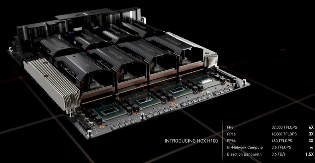
What is clear to us is that history is repeating itself because the DGX machines based on V100 and A100 GPU accelerators and using the first generation NVSwitch converged the memory on GPU sockets inside of the node into one shared, distributed address space and now, with the H100 generation and a new leaf/spine topology, NVSwitch is creating a federated GPU memory space that scales across 32 nodes. Doubling the raw performance of the GPU moving from the “Ampere” A100 to the “Hopper” H100 was important, but equally important is the new Tensor Core that is aimed at accelerating transformer models and that also has FP8 8-bit precision to boost the performance of the H100 by a factor of 6X on such models. But even that increase can’t make a single node shared memory system keep up, and as we suspected Nvidia would have to do four years ago, NVSwitch has to be itself transformed from a fast, dedicated in-node memory bus into a full-blown memory cluster fabric.
When NVSwitch was first announced four years ago, it was pulled out of Nvidia Research and productized rapidly (and way ahead of plan) because Nvidia needed to scale AI training models faster than any single GPU was scaling. And at the time, when we suggested that NVSwitch could be used to interlink multiple nodes together, Nvidia said that the best way to interconnect DGX nodes was to cluster the machines using many coupled InfiniBand interfaces to create a fat and fast pipe. But a switch is a switch and one that speaks GPU memory atomics is unique and useful, and we said at the time that we figured some OEM or ODM would be experimenting with how to interconnect nodes together using an NVSwitch fabric. Well, that didn’t happen, and probably because NVSwitch was only sold bundled inside of the HGX system boards as a complete unit.
The first NVSwitch, which was available in the DGX-2 platform based on the V100 GPU accelerators, had 18 NVLink 2.0 ports, each with eight lanes in each direction running at 25.8 Gb/sec speeds, which yielded a total of 25 GB/sec of bandwidth per port. There were two blocks of eight NVLink ports, connected by a non-blocking crossbar, plus two spare ports that were never explained. (We figured they would be uplinks to cluster switches.) That system had a dozen of the NVSwitch ASICs, six per HGX motherboard, and half of the links were used to hook the switch ASICs to the eight GPUs on the board and the other half were used to link to the other set of six ASICs on the second HGX board. There was 2.4 TB/sec of bi-section bandwidth between the two HGX boards, and any of the GPUs on any single board could communicate to any other GPU on that board at 300 GB/sec of bandwidth with one hop across the NVSwitch. It took three hops to get to the GPUs on the other HGX board.
With the DGX A100 system and its HGX A100 system boards, Nvidia needed to double up the bandwidth into the GA100 GPUs, and so it cut the scale of the NVSwitch fabric in half, to only eight GPUs, and pumped up those GPU to GPU links to 600 GB/sec. The total switch throughput was 7.2 Tb/sec, if you want to think about this the way switch ASIC makers do, and this was the aggregate switching capacity of the original NVSwitch. Nvidia calls the NVSwitch used in the DGX A100 systems and the HGX A100 boards its second generation, and the big change was to move to 50 Gb/sec signaling on the SerDes, which means it could put twelve NVLinks on each A100 and drive 600 GB/sec of bandwidth using the same number of NVLink lanes as the V100, which had six NVLink ports and topped out at that 300 GB/sec mentioned above.
With NVSwitch 3 – that is our name for it because Nvidia is calling it the third generation NVSwitch, which is too long – the aggregate bandwidth of the device is being boosted by 66.7 percent to 12.8 Tb/sec, and the NVLink 4.0 port speeds deliver 900 GB/sec of bandwidth into and out of the H100 accelerator using a total of 18 NVLinks, compared to the 12 links, and this can be done by only using two differential pairs in each direction rather than the four pairs used with the prior A100. The underlying signaling is running at 106.25 Gb/sec for NVLink 4.0. The internal NVSwitch 3 ASIC has 64 NVLink 4.0 ports and the external NVLink Switch has 128 NVLink ports and we believe has two of these NVSwitch 3 ASICs in the chassis; the bandwidth of 25.6 TB/sec – twice what the NVSwitch 3 specs are – backs this up:
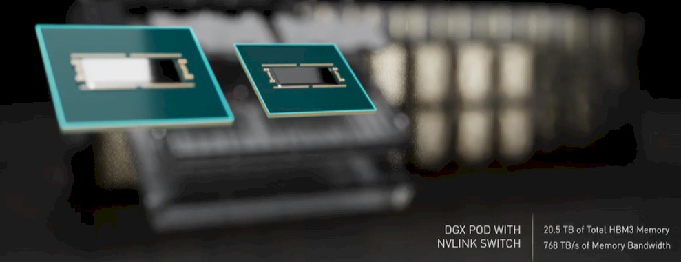
The NVLink Switch puts two of these packages into a single chassis:
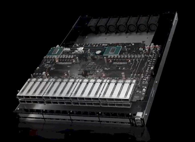
That chassis only shows 32 physical ports but it is supposed to have 128 NVLink ports. Perhaps this is due to link aggregation and then cable splitting? It is unclear.
One last thing about NVSwitch 3: Nvidia has ported the SHARP in-network computing algorithms and circuitry from its InfiniBand switches to the NVSwitch 3 ASIC, giving it the ability to do certain collective and reduction operations in the network. This is a big deal, as you can see from the capacity of compute now in the network:
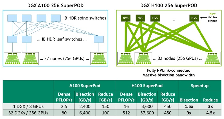
Here is how the networking stacks up to build the DGX H100 system, the DGX SuperPOD, and the Eos AI – and we think HPC – supercomputer.
The DGX H100 system only needs four of the NVSwitch 3 ASICs to cross couple the eight H100 GPU accelerators in the box to each other and still leave enough of NVLinks together to reach out to a second tier of NVSwitch boxes to glue up to 32 of the DGX H100 systems together into a shared system cluster. (By comparison, the DGX-2 needed twelve of the NVSwitch 1 ASICs to cross-couple sixteen V100 GPU accelerators inside the box and the DGX A100 needed six NVSwitch 2 ASICs to cross-couple eight A100 GPU accelerators.)
But check this out. Across that 32 node DGX H100 SuperPOD system – and they are sharing HBM3 memory on all of those GPUs, so it really is a system – there are 256 H100 GPU accelerators, but if you add up all of the switch ASICs, there are 164 of them. The network is 40 percent of the heavy chippery. With so many more ports and so much more bandwidth, now the internal NVSwitch 3 chips in the DGX H100 system can act as leaf switches in a left/spine network, and when 18 of these NVLink Switch external switches, which fit into a single rack in the center of the machine, are added, they just blow away the performance of the 100 Gb/sec HDR InfiniBand leaf/spine network that was used in the DGX A100 SuperPOD. Take a look:
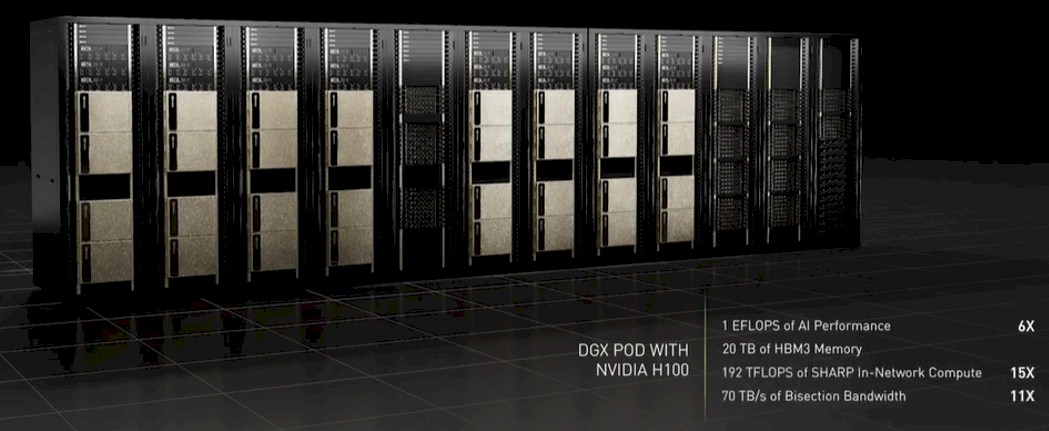
But that DGX SuperPOD is not big enough or fast enough for Nvidia. And that is why it is building the Eos supercomputer, shown in rendering below and to be built “in the next few months,” according to Jensen Huang, Nvidia’s co-founder and chief executive officer.
With Eos, Nvidia will couple together 18 of the DGX H100 SuperPODs to make a monstrous machine – one that would be ranked first or second in the world, depending on your level of precision. At the moment, it would beat the existing “Summit” supercomputer at Oak Ridge National Laboratory in the United States at FP64 math (as gauged by the Linpack benchmark) and it would best the “Fugaku” supercomputer at RIKEN Lab in Japan at reduced precision math.
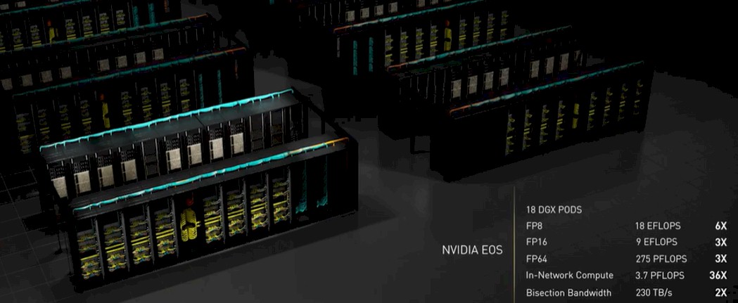
This beast has 576 DGX H100 systems with a total of 4,608 H100 GPU accelerators. By our count, the system has 2,304 NVSwitch 3 ASICs internally across those machines, and another 360 NVLink Switch enclosures with 720 of the NVSwitch 3 ASICs. There are 500 of the Quantum-2 NDR InfiniBand switches, so add another 500 ASICs there. Add it all up, and there are 3,524 switch ASICs in the Eos system, or 43.3 percent of the total 8,132 devices. (We can hardly count the CPUs in the DGX boxes because, computationally speaking, they are mostly doing housekeeping.)
This is not the kind of ratio of compute and networking that we see in HPC clusters or in hyperscale or cloud systems, either. Nvidia is bringing very serious networking, from both Nvidia and the former Mellanox Technology, to bear on solving the hardest scaling problems of our time.
We wonder how many HPC shops – particularly those who have an increasing AI workload – are going to look at what Nvidia has built and start getting a bit envious of the AI crowd. And we are sure that more than a few HPC centers – starting with CSCS in Switzerland – will look at the “Grace” Arm CPU complex and the Hopper GPU, and all of this NVSwitch memory interconnect, and start wondering what they might do with a very large shared memory cluster. Like the ones many had always dreamed of having so many years ago. All Nvidia has to do to scale this is add another NVSwitch network layer … or build a more capacious switch ASIC.
Even if Nvidia doesn’t want to be a prime contractor, its deep pockets and its technical prowess may mean it is pushed into this. HPC centers just won’t get the kind of deals they are used to. They can either pay more, or lose the leading edge to the hyperscalers and cloud builders, who absolutely can afford as many powerful machines as they want.


As CUDA Is To GPU, QODA is To Quantum Compute
In Nvidia’s decade and a half push to make GPU acceleration core to all kinds of high performance computing, a key component has been the CUDA parallel computing platform that made it easier for developers to create applications that can leverage graphics chips for general purpose processing. The GPU maker …
Nvidia Previews Ampere Kicker To Turing GPU Accelerator
We are still digging through the content coming out of the GTC 2020 fall conference and would be remiss if we didn’t talk a bit about the “Ampere” A40 and A6000 GPU accelerators that Nvidia is previewing. Nvidia has always designed distinct GPUs for different workloads, and some of them …
The AI Boom Props Up Datacenter Infrastructure Spending
If there is one thing that is absolutely immune from inflationary curbs and that is, to a certain degree, also contributing to inflationary pressures in the global economy, it is generative AI. In fact, from the limited data we have about server and storage spending in the world right now, …
Very impressive raw numbers. I would be interested to see real world benchmarks.
With networks of this scale, it’s often most interesting to know what the network performs like when 2 of the switches are disabled, 4 of the network cables are dead, and 2 of the network cables work, but are transmitting occasional malformed packets. That’s the way it’ll have to run, much of the time. Not to say that nvidia hasn’t thought of this, but it shows up in the real world numbers.
I presume there are spares sitting in most HPC and AI centers for this contingency, but it is a good point to make that what happens when you “chaos monkey” the network. I don’t know the answer, but it sounds like a good story to chase….
Back when Omni-path was the latest greatest, the switch here broke (during a vendor upgrade) leaving thousands of cores connected to each other only by means of the administrative Ethernet. Because the replacement switch was astonishingly out of stock this situation persisted for more than 6 months.
My guess is most of the small HPC clusters similarly rely on vendor service and warranties for big-ticket replacement parts rather than redundantly keeping their own on site.
The vertical integration that Nvidia has put together is not only useful from a performance point of view, but in these days of unreliable supply chains this type of vertical integration may allow Nvidia to more reliably take on the responsibility of delivering large systems according to contact.
Do Lenovo, Dell, HPE or even IBM have the needed level of control over their supply chains to provide the same practical delivery results as Nvidia? What about smaller companies such as Penguin?
And not just the vertical integration and the supply chain control, which are important. (As the shortages of Mellanox ConnectX adapters right now is causing all kinds of server delays….) But the fact that Nvidia is a big user of supercomputing, understands all of the headaches and builds the first system for itself and runs it before putting it out for sale means it has built the skills to do this. Is HPE or Dell or Lenovo or Atos a big user of supercomputing in the same way? I am not contending that Nvidia will want to be a prime contractor. I am thinking it will be forced into it.
And when the prime contractor stamps these as “Nvidia certified” there would be some rather hefty ongoing support contracts generated.