

Last May, after we had done a deep dive on the “Hopper” H100 GPU accelerator architecture and as we were trying to reckon what Nvidia could charge for the PCI-Express and SXM5 variants of the GH100, we said that Nvidia needed to launch a Hopper-Hopper superchip. The performance of the PCI-Express variant of the chip – and the expected gap in pricing – was such that we thought Nvidia might be tempted to repeat its history.
The “Kepler” K80 twofer GPU card, launched way back in 2014, came out because Nvidia was so focused on the exploding AI market that it didn’t put enough 64-bit floating point math in the follow-on “Maxwell” GPU, and the stopgap was to just put two K40s on a single card and go for the density play with a bit of a price break. (You can do that with workloads that scale out.)
For those customers who were not going to deploy the SXM5 version of the H100 GPU and its shared inter-node or extra-node NVLink memory switched fabric and who were going to just network the PCI-Express versions together using InfiniBand, an H100 twofer – call it the H200 – this made a lot of sense to us.
With the launch of the H100-NVL GPU today at the Spring 2023 GPU Technical Conference today, Nvidia is sort of doing what we expected. But not quite.
When we said a Hopper-Hopper package, we thought it would be something that looked like the Grace-Hopper CPU-GPU hybrid package or the Grace-Grace twofer package that Nvidia revealed this time last year during the initial Hopper launch at the Spring 2022 GTC. What we got instead with the H100-NVL is quite a bit different and quite a bit fatter, but in some ways better, than what we expected, and hopefully it is also considerably cheaper than what we think Nvidia is charging for the full-on H100 SXM5 GPU accelerators.
The H100-NVL two PCI-Express versions of the GH100 GPU with slower HBM2e memory, with the GPUs not on a single, shared package but rather on two adjacent cards using a trio of NVLink 4.0 ports lashing the high bandwidth memories of the two GPUs together.
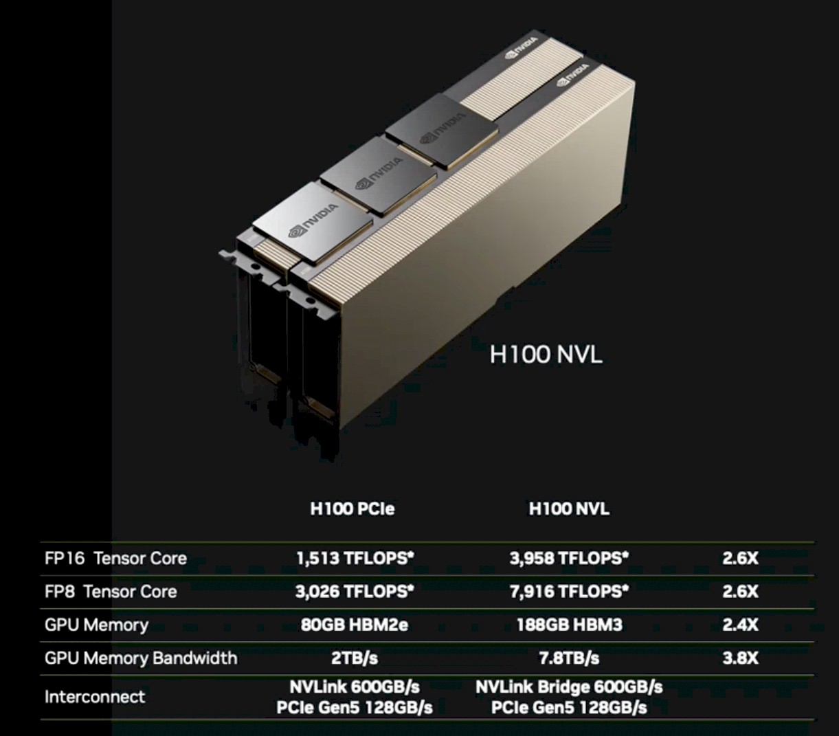
That the H100-NVL has moved the PCI-Express version over to full HBM3 stacked memory, up from HBM2e memory running in the single-wide PCI-Express version of the H100 accelerator launched last year. This quadruple-wide card has 94 GB of memory per GPU, up from 80 GB per GPU with both the PCI-Express and SXM5 versions (which add NVLink interconnects out of the GPUs to hook in an eight-way NVSwitch NUMA complex across the GPUs in a single node.) On the 80 GB HBM devices, there are five out of six possible HBM stacks operating, and they have 16 GB each. (The sixth is dead to increase yield.) With the H100-NVL twofer, the memory is not only boosted by 20 percent to 94 GB per GPU, but the memory speed on the HBM3 stacks is also goosed by 33 percent, yielding 3.9 TB/sec of bandwidth per GPU, which is twice the 1.95 TB/sec that the double-wide H100 PCI-Express 5.0 card offered last year with its 80 GB of HBM2e memory.
On the compute front, the H100-NVL has the same GH100 GPU as the H100 SXM version, which has had its official performance ratings boosted at some point in the past year by a tiny bit. And it puts two of them on adjacent pairs of PCI-Express mountings, all packaged up as a single device, four of which can fit inside of a DGX server frame or indeed any other 5U frame that has been created to host A100 or H100 GPUs. There is absolutely no density advantage to using the H100-NVL – two GPUs take up twice the space of a single GPU from last year, which is no gain – but the increased performance in the PCI-Express form factor, at 31.3 percent higher per unit of volume, will be appealing, and so will be the extra 17.5 percent memory capacity and the doubling of memory bandwidth per GPU over the single H100 PCI-Express card.
In fact, when we look at the H100-NVL device, we see some companies looking at this for AI training, not just the AI inference that Nvidia executives talked about in prebriefings about the new device.
What companies do depends to a certain extent on what Nvidia will charge for the H100-NVL device, and we have no idea what the plan is there. But given that it is focusing this device on inference, and specifically the big fat inference that is necessary to run foundation model inference with hundreds of billions of parameters, we think Nvidia will have to walk a fine line so it does not make inference so expensive that it drives it off to CPUs.
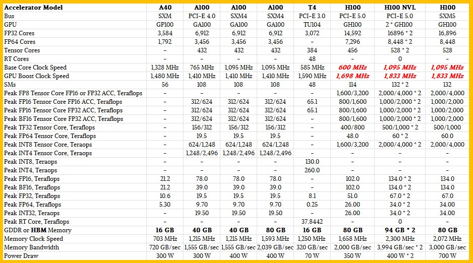
Here is how the H100-NVL stacks up to other Hopper GPUs as well as relevant ones from the “Turing” and “Ampere” generations that are used for both AI inference and AI training:
To make the point that the H100-NVL was aimed at inference workloads, Ian Buck, vice president of hyperscale and HPC at Nvidia, said that doing inference on the GPT-3 foundation model with 175 billion parameters, a single H100-NVL had 12X the throughput of an “Ampere” A100 GPU accelerator. The raw performance difference between the FP8 processing on the H100-NVL, at 8,000 teraflops, and the INT8 performance of the A100, at 1,248 teraflops, is only 6.4X in the data we have, so there is something weird about scaling GPT-3 175B we presume.
The other new GPU announced today at GTC Spring 2023 is the L4 GPU, which is based on the “Lovelace” AD104 GPU, a companion to the Lovelace AD102 GPU that was unveiled in the L40 GPU accelerator last September.
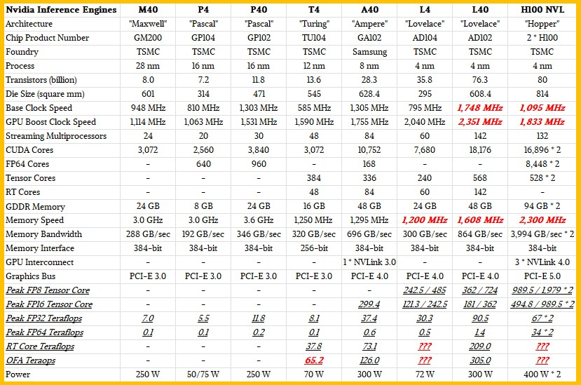 The L4 GPU accelerator, like its P4 and T4 predecessors, is mean to fit in a 75 watt or smaller power envelope and is meant to handle AI inference as well as graphics and video encoding workloads in the datacenter. The data is a little thin on the L4 in particular, but there are feeds and speeds out there on the Internet for the AD104 GPU and we have done our best to fill in the gaps in the comparison table above.
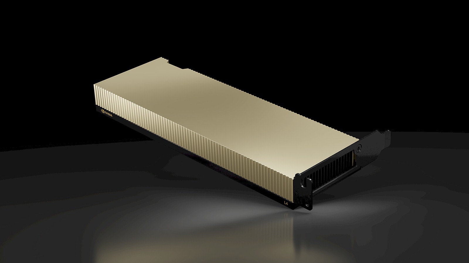
The L4 card plugs into a PCI-Express 4.0 x16 slot so it can be deployed in servers that have been in the field for a number of years already – not so much because companies will put them into existing machines, but rather use existing, certified platforms to build inference servers rather than go get the latest X86 servers that have PCI-Express 5.0 slots that would be all the more skinny. Eventually there will be an L40 x8 device on the PCI-Express 5.0 bus, or an L45 or some future thing like that.
Using Stable Diffusion’s generative AI image processing atop the TensorRT stack, the L4 was able to do 2.7X the work of an earlier generation T4 device when it came to image inference. For video encoding – which is a big deal for the hyperscalers and cloud builders – the L4 can do double-time as a video encoding platform (and one with Ai assistance to boost resolution). Nvidia says that a DGX server with eight of the L4s can do 120X the world of a two-socket “Ice Lake” Xeon SP-8362.
With that, Nvidia now has four different inference platforms that it sells and that OEMs and ODMs use as inspiration for their own designs:
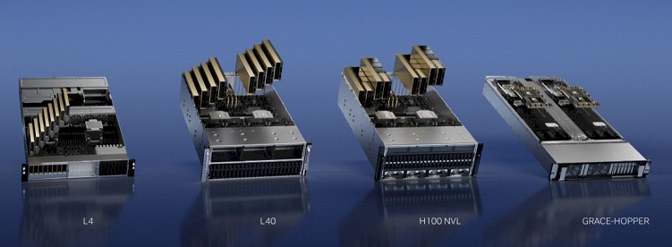
Depending on how you feel, these are the four workhorses of the AI inference revolution or the four horses of the AI pockyclypse. The truth is probably somewhere in the middle, which is where you can usually find it.
We plan to have a looksee with OEMs and resellers to see how the H100s, L4s, and L40s are being priced out there in the market, and how prior A40s, T4s, and A100s are priced, and will report back when we learn something of use.


I guess the stated 12x speedup of the H100-NVL (vs the 6.4x that you calculate) is a comparison of its FP8 performance to the FP16 perf of the A100 — which is a bit misleading — but, overall, these H100/GH100 devices are quite impressive!
Quite remarkable that British outfit Plumerai successfully does AI inferencing for real-time people detection in video streams on puny microcontrollers, like Cortex-M0 (hopefully not to be confused with the French “je te plumerai”, meaning “I will fleece you”). Accordingly, I would hope to see the four horses (L4 to G+H) finding uses in training as well, not just inferencing, given their awesome oomph! Meanwhile, we’ll celebrate the 50th anniversary of the dystopian no-future anthem in 2027, noting how Johnny Rotten’s brother Ralph, while enjoying a calizona in anti-gravity, posited the pockyclypse, near one of TSMC’s Arizona fabs, likely the one etching those GHB100 chips, with DDR13 viral memory. Whether such positioning turns out to be literally literary humor, of quick, shell, or bubble sorts, obviously remains to be ascertained (eh-eh-eh)!
I will pluck your feathers? HA!
Admittedly, my French is merde….
What a bullshit marketing. Inference of huge models is much cheaper on CPUs and it is mostly in interest of very few who host solutions like ChatGPT. For most people (researches) the most important is training performance. And for this most important is memory bandwidth. I don’t understand who NVIDIA is trying to target with “Inference Revolution”, they try to bullshit researches?
As of Ada and Hopper there appear to be no option for training from nVidia other than the most expensive card. 4090 has no nvlink and will not work with NCCL P2P, same for RTX 6000 Ada. Many outfits do not have workloads that map onto multiprecision H100, many outfits cannot afford them anyway.
I don’t understand Jen Sen’s thinking. Outside gov’t labs and the hyperscalars he has priced and de-featured nVidia out of the market.
It is a terrible situation. I was hoping to upgrade my RTX A6000 pair to RTX 6000 Ada, but it without P2P multi GPU training is ruled out, and the price has about doubled anyway.
AMD isn’t even trying to compete, PCIe Mi2x0 is effectively unavailable and RX 7000 cards are a crapshoot for HIP support. This is the end of an era of small agile competition and innovation.