
We have said it before, and we will say it again right here: If you can make a matrix math engine that runs the PyTorch framework and the Llama large language model, both of which are open source and both of which come out of Meta Platforms and both of which will be widely adopted by enterprises, then you can sell that matrix math engine.
With Intel unveiling its third generation Gaudi AI accelerators today at its Vision 2024 event in Phoenix, where the company has big foundry operations nearby Chandler, the only questions, then, are how many Gaudi 3 accelerators can Intel make, what will it charge for them, and when can it ship them?
The first question is something that only Intel, which is working with Taiwan Semiconductor Manufacturing Co to etch and package the Gaudi 3 accelerators, knows. Habana Labs, which was acquired by Intel in December 2019 for $2 billion, launched the Gaudi 1 accelerator back in July 2019, which was when Nvidia’s “Volta” V100 was the competition in a ridiculously smaller AI space. Hopefully Intel will be more aggressive in making and selling Gaudi 3 chips than it has been with either Gaudi 1 or Gaudi 2, even if it will soon be significantly behind Nvidia when it comes to raw accelerator performance. There is a chance for Intel to be aggressive and attract the PyTorch crowd, with Llama LLMs and a seemingly zillion other AI models available on Hugging Face.
This is enough to build the foundation of an AI accelerator business – provided that customers trust there will be enough architectural similarities between Gaudi 3 and the hybrid CPU/NNP design that is coming with “Falcon Shores” out in late 2024 or early 2025 or so. That launch date for Falcon Shores, which will sport a variant of HBM3 memory, depends on how you want to read the vague roadmap Intel has published for Gaudi line. What we do know is that Falcon Shores merges the Gaudi line with the Max Series GPU line to create a GPU that has the Ethernet interconnect and matrix math tensor cores of Gaudi combined with the Xe vector engines of a “Ponte Vecchio” GPU.
As for the cost of the Gaudi 3 accelerators, the answer is simple. Intel’s price will be directly proportional to the performance of the Nvidia “Hopper” H100 GPU accelerator that it completes against and the street price that Hopper H100 GPUs have with 96 GB of HBM3 memory capacity and 3.9 TB/sec of bandwidth. As the Hopper H200 variants, which have 141 GB of HBM3e memory capacity and 4.8 TB/sec of bandwidth, start shipping in a few months, the math will shift to a comparison with the H200s. And when the future “Blackwell” B100 and B200 GPU accelerators start shipping from Nvidia later this year and into 2025, the Gaudi 3 price will have to adjust accordingly.
Is The Third Time The Charm?
It would have been better for Intel, obviously, if the Gaudi 3 accelerator was launched in the spring of 2022 alongside the Hopper GPU, and in appreciable volumes at that. Here we are two years later, and demand for Nvidia GPUs is so strong that there is never a better time to sell a technology that should already be two years old. Better to launch it now than not launch it at all, and at this point, it would be better to get Falcon Shores into the field sooner rather than later.
Intel can sell all of Gaudi 3 and Falcon Shores that it can make in the short term. Now is the time to hustle. The timing for Gaudi 3 and Falcon Shores could have been better, but any delays in ramps means billions of dollars in systems sales being deferred and possibly lost as Nvidia ramps mightily and AMD starts getting traction, too, with its “Antares” Instinct MI300 series of GPU accelerators.
The Gaudi 3 accelerator is an big evolutionary jump from the Gaudi 2. But the big architectural change is coming with Falcon Shores, but one that will largely be insulated from customers using PyTorch and higher models upon that framework. It would have been good for Habana Labs and then Intel if Meta Platforms had chosen the Gaudi accelerators as its AI engines, but clearly that did not happen and the social network is creating its own line of MTIA accelerators for AI training and inference and in the interim is buying hundreds of thousands of Nvidia GPUs.
Let’s walk through the Gaudi 1 and Gaudi 2 architectures and then take a look at the Gaudi 3 accelerator, the system designs using it, and the various packagings for Gaudi 3 that Intel will bring to market. We will do a separate story comparing the price/performance of current Nvidia and AMD GPUs to the Gaudi 3 line.
Made To Do Math
As is the case with other AI accelerators that include matrix math units and tensor cores (which are a special kind of matrix math unit), the original Gaudi 1 accelerator could in theory be used to accelerator other kinds of workloads, including HPC simulation and modeling and even data analytics. It is just a matter of creating the software stack for it. But in this case, as is also the case with other mixed precision AI accelerators, the availability of mixed – and importantly, low precision – floating point and integer math makes is most suited to AI training and inference.
The Gaudi 1 accelerator and software stack that Habana Labs put together, which compelled Intel to buy the company even though it had previously bought AI accelerator maker Nervana Systems for $350 million back in August 2016. (Intel didn’t productize the Nervana NNPs until November 2019, and a month later it bought Habana Labs. Go figure.)
Here is the block diagram of the Gaudi 1:
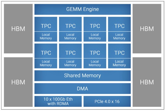
The architecture includes a generic GEMM Engine matrix math engine, plus eight tensor processing cores (TPCs) with their own local memory. The GEMM Engine did the math operations for fully connected layers, convolutions, and batched GEMM processing in integer format at 16-bit precision, while the TPC is a special SIMD processor made to handle other machine learning operations. The TPCs process data in FP32, BF16, INT32, INT16, INT8, UINT32, UINT16, and UINT8 formats.
The SRAM memory shared by the TPCs (and presumably also the GEMM unit) weighed in at 24 MB and had 1 TB/sec of bandwidth; the size and the bandwidth of the local memories on the TPCs was never divulged as far as we know.
The Gaudi 2 was etched in TSMC’s 16 nanometer process and used 2.5D CoWoS packaging to link four stacks of HBM2 memory, at 8 GB per stack, for a total of 32 GB of memory with 1 TB/sec of aggregate bandwidth. The chip also had ten 100 Gb/sec Ethernet RoCE ports to interconnect Gaudi processors within a server node and across server nodes in a cluster, with a maximum of 128 fully connected nodes. The device also had a PCI-Express 4.0 x16 controller to reach out to host CPUs.
With the Gaudi 2, which launched in May 2022 and which started shipping in volume and on the Intel Developer Cloud in June 2023, the Habana team inside of Intel cranked it all up, thanks in large part to a move to TSMC’s 7 nanometer etching.
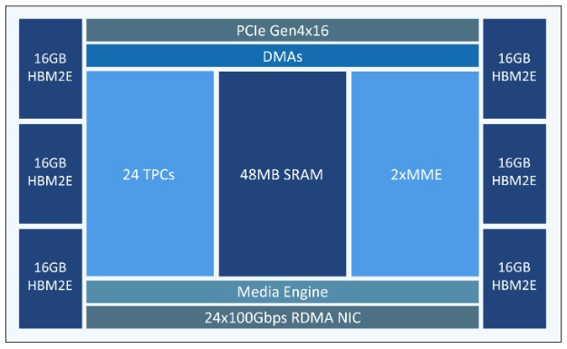
The shared SRAM memory was boosted from 24 MB to 48 MB. The number of TPCs was increased by 3X to 24 units, and the number of GEMM units – now called the Matrix Math Engine – was doubled. The Ethernet port count went up by 2.4X to 24 ports, which radically increased the scalability of Gaudi clusters, and media decoders were added to do pre-processing for AI vision applications. The TPCs supported FP32, TF32, BF16, FP16, and FP8 (both E4M3 and E5M2 variations) data formats. The MME unit does matrix math and accumulates to FP32 format, according to the documentation. (It is not clear if the GEMM is the same as the MME. But if so, it does matrix math on 16-bit integers and accumulates to 32-bit floating point.) The Gaudi 2 has the same PCI-Express 4.0 x16 link out to hosts, but has six HBM2E memory controllers and six HBM2E memory stacks at 16 GB each, for a total of 96 GB of capacity and 2.4 TB/sec of bandwidth across those six stacks.
That brings us to Gaudi 3 and the shift to TSMC 5 nanometer etching.
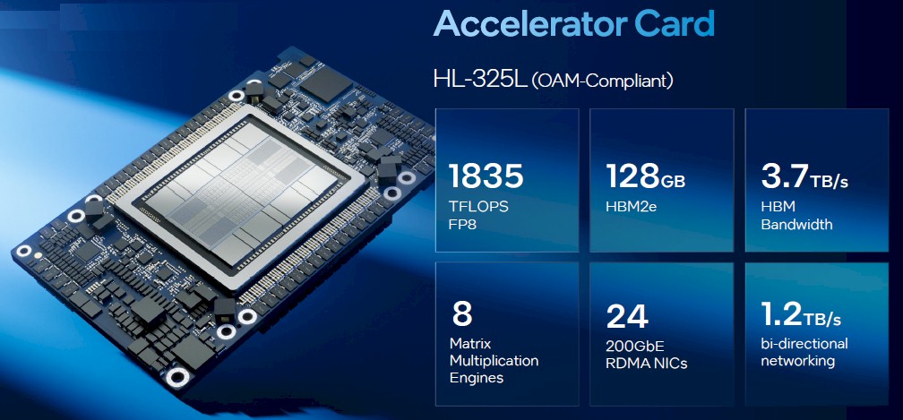
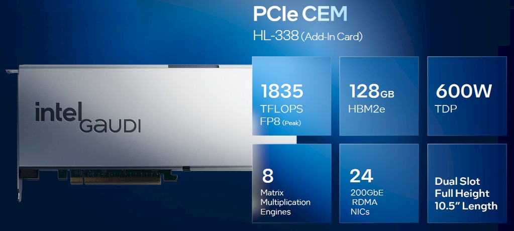
Here is what the Gaudi 3 accelerator looks like:
And here are the specs:
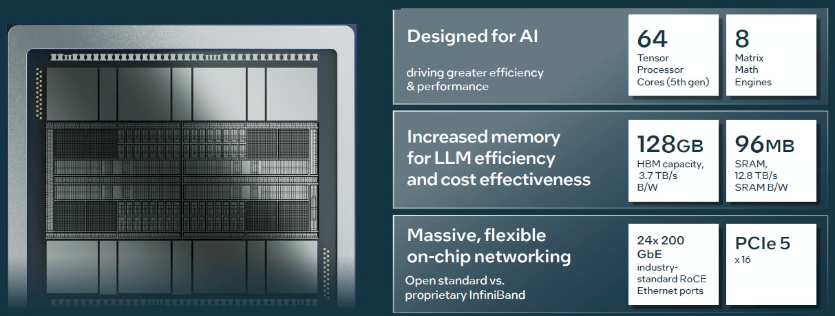
The Gaudi 3 is a much beefier device. The TPC design is in its fifth generation, according to Eitan Medina, chief operating officer at Habana Labs, who has that same role inside of Intel. There are 64 of these TPCs on the Gaudi 3 device, which is an increase of 50 percent over the Gaudi 2. There are also eight MMEs, a factor of 4X more than the Gaudi 2.
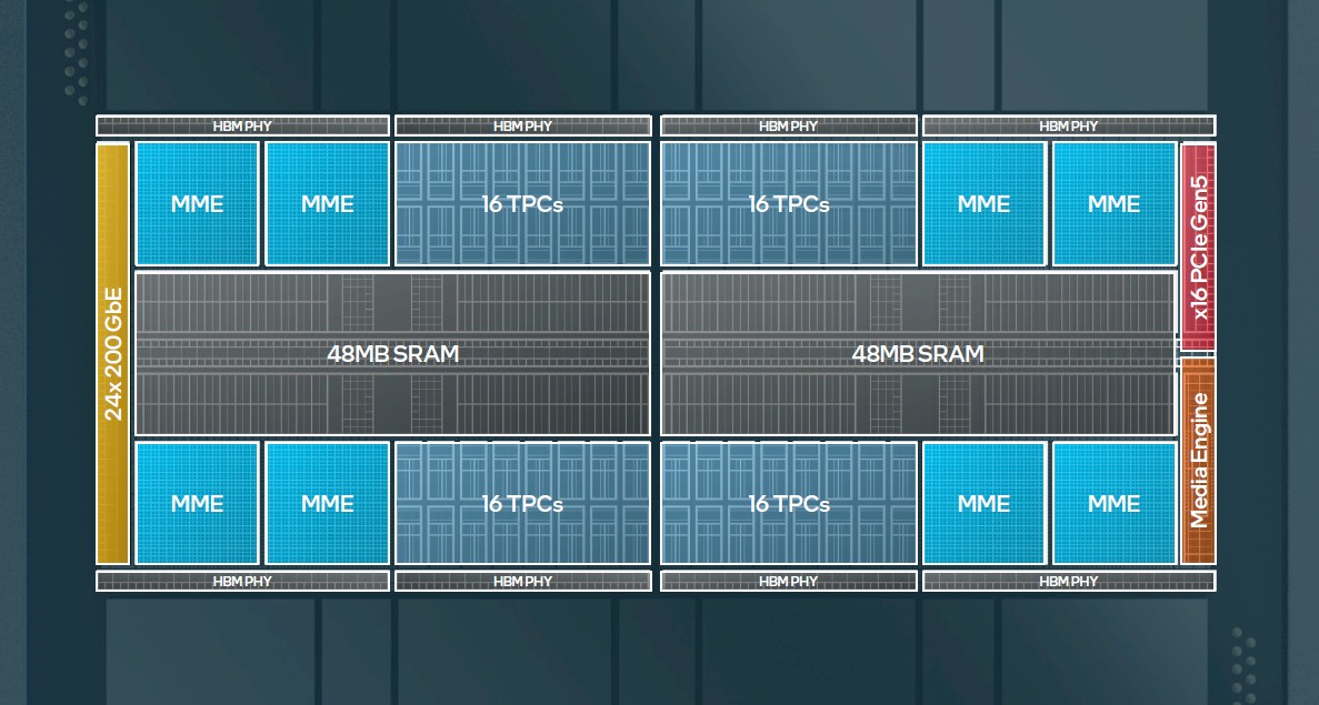
This is a simplified diagram, according to Medina, but as you might expect these days, there are two identical Gaudi 3 chiplets that are rotated 180 degrees from each other that implement half of the two dozen 200 Gb/sec Ethernet ports, half of the media engines, and presumably one PCI-Express 5.0 x8 port for each tile that presumably can be ganged up to make a single virtual PCI-Express 5.0 x16 port shown on the simplified block diagram.
There is 48 MB of SRAM shared memory on each Gaudi 3 tile, and two blocks of 16 TPCs and two blocks of two MMEs. The 96 MB of SRAM has 12.8 TB/sec of aggregate bandwidth inside the Gaudi 3 complex. There are eight HBM2E memory stacks with a total of 128 GB of capacity and 3.7 TB/sec of bandwidth.
As far as we know, the TPCs in the Gaudi 3 device support the same FP32, TF32, BF16, FP16, and FP8 data formats as Gaudi 2 does, and does not support FP4 precision as the new Blackwell GPUs from Nvidia will and that the existing Hopper GPUs from Nvidia do not.
Scaling Up Gaudi 3 In A Node And Out Across A Cluster
An AI accelerator is only as good as the clusters that can be built from it, and as has been the case from the beginning, the Gaudi team is integrating Ethernet juiced with RDMA and other lossless features in the RoCE protocol extensions to get it done without InfiniBand.
Here are the speeds and feeds of clusters at the FP8 precision that is sometimes used for AI training and that is increasingly being used for AI inference:
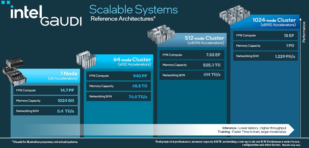
An eight-way Gaudi 3 node is rated at 14.7 petaflops at FP8 precision, and an eight-way Hopper H100 node is rated at 15.8 petaflops at FP8 precision without 2:1 sparsity support turned on. That is spitting distance given that not all applications can support that 2:1 sparsity. (With dense matrices, sparsity support don’t do nothing.) Those original H100s from Nvidia also had only 80 GB of HBM3 capacity but 3.35 TB/sec of bandwidth. Intel is getting more capacity and more bandwidth by sticking with cheaper HBM2E, which is interesting. The H200 from Nvidia has 141 GB of HBM3E and 4.8 TB/sec of bandwidth, which is 10.2 percent more memory capacity and 29.7 percent more bandwidth. (Ah, but at what price? The additional cost of a Grace CPU maybe?)
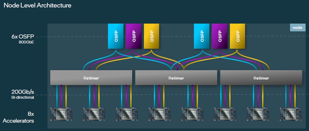
The Gaudi 3 accelerators inside of the nodes are connected using the same OSFP links to the outside world as happened with the Gaudi 2 designs, but in this case the doubling of the speed means that Intel has had to add retimers between the Ethernet ports on the Gaudi 3 cards and the six 800 Gb/sec OSFP ports that come out of the back of the system board. Of the 24 ports on each Gaudi 3, 21 of them are used to make a high-bandwidth all-to-all network linking those Gaudi 3 devices tightly to each other. Like this:
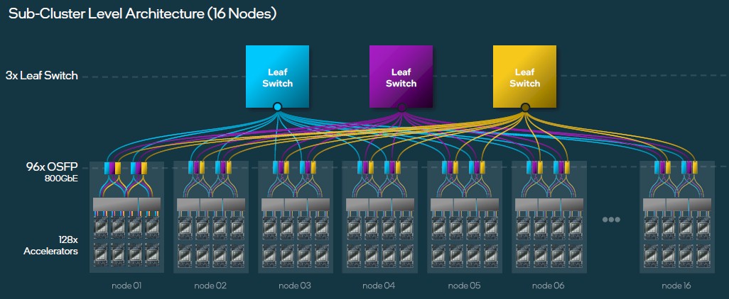
As you scale, you build a sub-cluster with sixteen of these eight-way Gaudi 3 nodes, with three leaf switches – generally based on the 51.2 Tb/sec “Tomahawk 5” StrataXGS switch ASICs from Broadcom, according to Medina – that have half of their 64 ports running at 800 GB/sec pointing down to the servers and half of their ports pointing up to the spine network. You need three leaf switches to do the trick:
To get to 4,096 Gaudi 3 accelerators across 512 server nodes, you build 32 sub-clusters and you cross link the 96 leaf switches with a three banks of sixteen spine switches, which will give you three different paths to link any Gaudi 3 to any other Gaudi 3 through two layers of network. Like this:
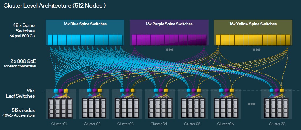
This chart should have labeled those as Sub Clusters, not Clusters. But you get the idea.
Now let’s touch on performance briefly, which we will get into in more depth separately. Medina showed off performance results that showed the Gaudi 3 was between 1.4X and 1.7X faster at training Llama2 7B and 13B and GPT-3 175B models than the Nvidia H100, and anywhere from 90 percent to 4X the performance of the H100 on inferencing with Llama 2 7B and 70B and Falcon 180B.
Form Factors Follow Function
That leaves us with the form factors. Here is the OAM version of the Gaudi 3 accelerator, which in theory should be preferred by Microsoft and Meta Platforms, who created the OAM form factor and open sourced it back in March 2019. Take a gander:
And here is the universal baseboard that takes eight of these and creates a single motherboard with all of those Gaudi 3 devices interconnected and six OSFP ports running at 800 Gb/sec to the outside world:
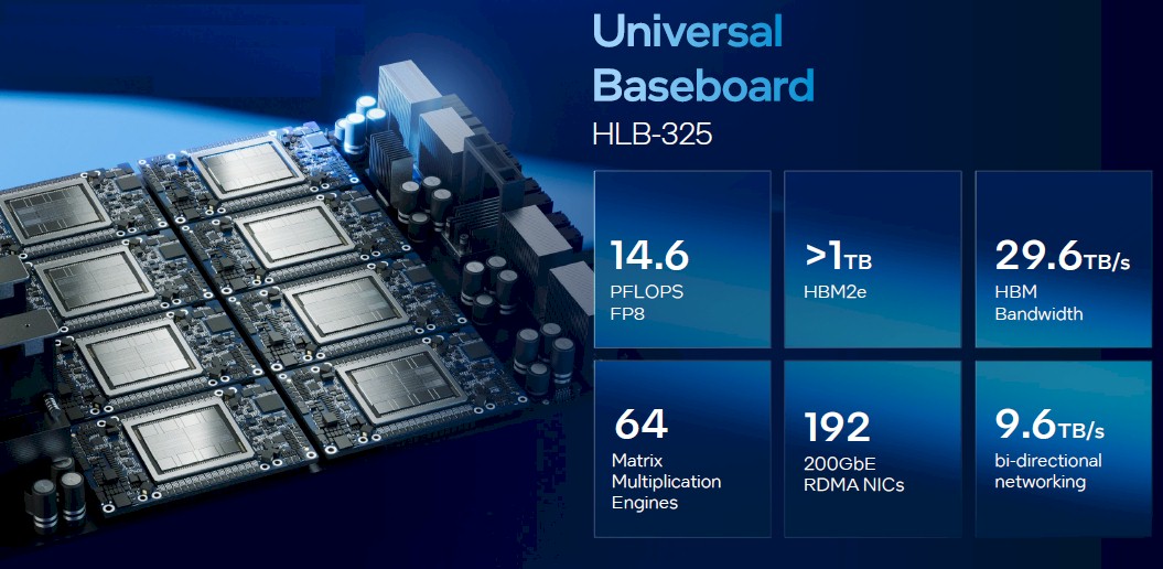
This UBB system is roughly analogous to Nvidia’s HGX system boards, which have been used for its A100, H100, and soon its B100 accelerators.
Intel is also going to deliver a PCI-Express 5.0 x16 variant of the Gaudi 3, with passive cooling so it can be plugged directly into any servers that support those slots in a dual-width form factor:
The air-cooled Gaudi 3 devices with those massive skyscraper heatsinks have been sampling for a few weeks and the liquid-cooled ones with cold plates mounted on them are sampling here in Q2 2024. The air-cooled Gaudi 3s will be in volume production in Q3 and the liquid-cooled ones will be in volume production in Q4. Dell, Hewlett Packard Enterprise, Lenovo, and Supermicro have all committed to make OEM systems based on these Gaudi 3 accelerators, and Gaudi 3 will also be available through the Intel Developer Cloud. Gaudi 2 was only in machines built by Supermicro. So the OEMs are taking Gaudi 3 more seriously than they did Gaudi 2 — and that has a lot to do with the low allocations the OEMs got during the Hopper GPU rollout.

With VMware, Broadcom Has A Real Enterprise Software Stack
Once Dell spun out VMware on Wall Street, it was only a matter of time before someone would put together enough money to acquire it. A year ago, we mused about Intel being the logical buyer of VMware once Pat Gelsinger left the top job at VMware to return to …
Finally: Some Good News For The Intel Xeon CPU Roadmap
It was a reasonable enough gut reaction given the many changes happening at Intel in recent months. The chip designer and maker – the last one in the world that does both – had announced a datacenter product line update for Wall Street analysts only a week after Raja Koduri, …
Tuning Up Nvidia’s AI Stack To Run On Virtual Infrastructure
Having to install a new kind of systems software stack and create applications is hard enough. Having to master a new kind of hardware, and the management of it, makes the situation worse. And for normal enterprises, this makes embracing AI in its many forms difficult. Enterprises looking to embrace …
Seeing how capable this Gaudi 3 is (a bit more than twice Gaudi2, or 4x Gaudi1), I got to wonder what Intel still needs Falcon Shores for (why not Gaudi 4, 5, 6, …)? But then, reading this article, it dawned on me: it doesn’t have FP64! Merging the Xᵉ GPU Max’s FP64 vector engines with Gaudi’s FP32-FP16-FP8 tensor and matrix units will likely be challenging, but is needed to fully compete with the MI300s and GB200s of the world. The result should be most interesting IMHO.
The absence of Gaudi4,5,6 in the roadmap may work against Gaudi3 to some extent. It is too risky for Intel to abandon Gaudi line for unknown ‘Shores’