

If you want to take on Nvidia on its home turf of AI processing, then you had better bring more than your A game. You better bring your A++ game, several vaults of money, and a few bags of good luck. Maybe a genie in a bottle would help, too.
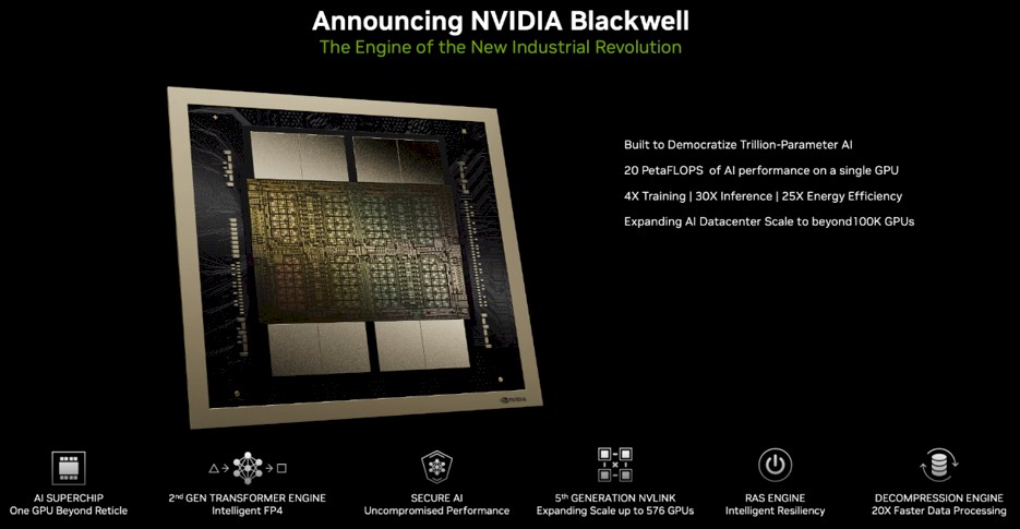
The launch of Nvidia’s “Blackwell” GPUs today at the 2024 GPU Technical Conference in San Jose represents the seventh and most impressive generation of datacenter class GPUs from the compute engine maker. This GPU computing wave started in the mid-2000s, but really started to crystalize with the launch of the “Kepler” K10 and K20 accelerators in May 2012.
And since that time, Nvidia has relentlessly driven Moore’s Law advances in transistors, advanced packaging, embiggening vector and matrix math engine designs, ever-reducing floating point math precision, and enfattening memory capacity and bandwidth to create compute engines that are 4,367X faster in terms of raw floating point performance than the base K10 with two GK104 GPUs was a dozen years ago. (And 8X of that performance jump is coming from reduced precision from FP32 single-precision to FP4 eighth precision floating point math, so the chip performance gain at constant precision is 546X.
And with advances in NVLink networking, hyperscalers, cloud builders, HPC centers and others can couple the memory and compute of hundreds of GPUs together tightly and with the advances in InfiniBand and Ethernet networking can lash together tens of thousands of GPUs together more loosely to build immensely powerful AI supercomputers that can also run HPC and data analytics workloads a whole lot faster, too.
How much faster the “Blackwell” B100 and B200 GPU accelerators are than their predecessor “Hopper” H100 and H200 GPUs that were launched in 2022 and 2023, respectively, remains to be seen. A lot of the architectural and performance details have yet to be divulged as we write this slightly ahead of the keynote presentation by Nvidia co-founder and chief executive officer Jensen Huang. We will be doing a follow-up story on the systems using the Blackwell GPUs and the usual architectural and economic deep dives on the new GPUs, stacking them up against their predecessors at Nvidia and the compute engines from AMD, Intel, and others.
AI Is Firmly In The Architectural Driver’s Seat
If the needs of the HPC sector for more floating point performance and lower energy consumption for that performance drove Nvidia’s initial compute designs, it has been clear since half precision FP16 units were added with the “Pascal” generation in 2016 and then tensor cores matrix math engines were added with the “Volta” generation only a year later in 2017 that machine learning workloads – specifically, deep learning neural networks – have been driving Nvidia’s architectural choices.
And with the Hopper and now Blackwell compute engines, the large language models that support generative AI are pushing the architecture even harder to drive down the cost of doing ever-larger AI training and inference workloads.
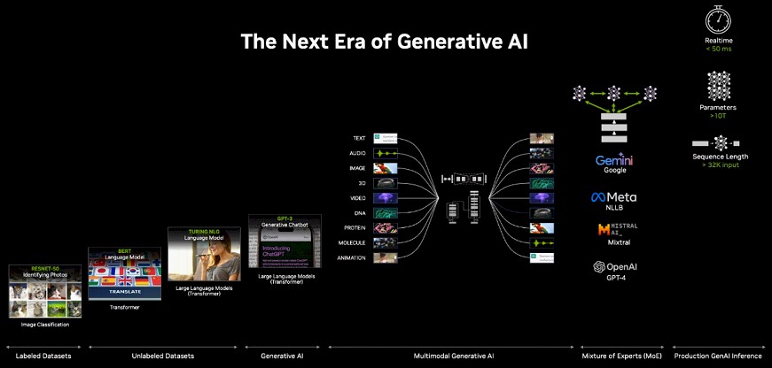
“Last year in 2023, we experienced the birth of multimodal generative AI, where text talks to image images, images can create texts, audio can create 3D – and not just in human modalities, but in areas of science of such as weather or DNA, molecules, and proteins and drug discovery,” explained Ian Buck, vice president of hyperscale and HPC at Nvidia, said in a prebriefing ahead of the conference. “A new kind of AI is emerging as a result. One that is even more intelligent, one that’s been built not just a single AI model, but as a collection of AI models, called a mixture of expert models – like Google Gemini or Meta NLLB or Mistral AI and of course OpenAI GPT-4. These new models actually take multiple AI models and have them operating in concert. And for every layer of a transformer, they are sharing their information to decide who has the best answer for the next layer to build even more intelligent models. This allows AI to scale further – to trillion parameter models – that we have never seen before. Of course, the challenge of that is computing. As models are getting larger, training takes more compute. Also, inference is becoming a bigger and bigger part of the challenge.”
Blackwell, in its various guises, is meant to address all of these challenges better than Hopper could.
(This seventh generation of true GPU compute engines is named after David Blackwell, a member of the National Academy of Sciences and a former professor at the University of California at Berkeley who did research in game theory, information theory, and probability and statistics.)
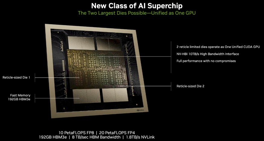
The Blackwell GPU complex has 208 billion transistors and is etched with a tweaked version of the 4 nanometer process from Taiwan Semiconductor Manufacturing Co called N4P, which is a refined version of the custom N4 process that was used by Nvidia to etch the Hopper GPUs. The Blackwell device is actually comprised of two reticle-sized GPU chips, each with 104 billion transistors, that are lashed together using NVLink 5.0 interconnects along the middle of the dies, like a zipper stitching them together.
Because Nvidia was unable to use TSMC’s 3N 3 nanometer process, which still has some kinks in it apparently and which were talked about nearly three years ago, we think the Blackwell chips are a bit bigger and hotter than they might have otherwise been. They might be running at slightly slower clock speeds, too. But each Blackwell die is going to pack about 25 percent more floating point oomph than a Hopper die does, and then there are two of them in each package for a combined 2.5X increase in performance. Dropping down to FP4 eighth precision floating point processing will double it up again to a 5X boost in raw performance. The actual performance on workloads could be higher depending on memory capacity and bandwidth configurations on various Blackwell devices.
Buck says that there are six core technologies that have made the Blackwell GPUs, which will ship later this year, possible:
Those two Blackwell dies are zippered together with a 10 TB/sec NVLink 5.0 chip to chip link, called the NV-HBI and presumably short for High Bandwidth Interconnect. And importantly, Buck confirms that these two chips present a single GPU image to software and are not just two GPUs sitting side-by-side, as has been the case with prior GPUs from both Nvidia and rival AMD.
This is important because if a device looks like a single unit, it is programmed line a single unit and the network talks to it like a single unit, and therefore it is the unit of scale across the cluster. If this were not true, then a cluster will not scale as far as you might think it can. (How badly the scale is impaired would depend on the way the network talked to each die, but in the best case scenario of a bad situation, it would cut the cluster’s compute scale in half.)
We don’t many specific feeds and speeds for the B100 and B200 devices, but we do know that the top-end Blackwell with all of its features turned on – and don’t assume that this will be the case with the B200 – currently has 192 GB of HBM3E memory.
But as you can clearly see, there are four banks for each of the Blackwell chips in the package, for a total of eight banks, and the Blackwell GPUs almost certainly use 4 GB DRAM chips that are stacked up eight high for a total of 64 chips. If you look very carefully at the die, you can see that it is really eight compute complexes packaged up across those two Blackwell dies, a one to one pairing with banks of HBM3E memory that is the right kind of symmetry as far as we are concerned. The combined memory bandwidth of that 192 GB of memory, which is being sourced from both SK Hynix and Micron Technology, as we previously reported three weeks ago in He Who Can Pay Top Dollar For HBM Memory Controls AI Training, is 8 TB/sec.
The H100 from 2022 had 80 GB of memory and 3.35 TB/sec of bandwidth across five stacks, and an upgraded H100 that was paired with the “Grace” CG100 Arm server processors also made by Nvidia came out with six stacks at 96 GB and 3.9 TB/sec of bandwidth. If you want to be generous in your comparisons, then you compare to the original H100, and the top-end Blackwell will have 2.4X the memory and 2.4X the bandwidth. If you compare to the middle H100 with all the memory turned on, then the increase for the top-end Blackwell that Nvidia is promising to deliver this year is 2X for capacity and a little more than 2X for bandwidth. If you compare to the H200 with 141 GB of HBM3E memory and 4.8 TB/sec of bandwidth, then the capacity on the top-end Blackwell is 36.2 percent higher but its bandwidth is 66.7 percent higher.
There is a chance that Nvidia could move to higher stacks with future Blackwell GPUs and boost the memory capacity further, but such a move would not yield an increase in bandwidth because there would only still be eight HBM3E memory controllers on the dies.
Note: We had originally went down a rat hole of math suggesting that only six of the eight HBM3E stacks were yielding and working to get to that 192 GB. (There is something about a 3 GB memory chip that violates our sensibility whereas a 4 GB chip does not.) If this were true, that would mean the Blackwell package could be upgraded to 256 GB of HBM3E capacity and 13.3 TB/sec of bandwidth at some point and that the current Blackwell HBM3E stacks would be driving at 1.33 TB/sec each. We had a rethink after some chats with readers and have scrubbed that idea of using 4 GB HBM3E memory and only having six stacks and are sticking with our analysis from back in July 2023. That said, with Micron saying it can drive more than 1.2 TB/sec out of a 24 GB stack, we think there is some bandwidth that can be added to future Blackwells while still sticking to HBM3E. That would be at least a 20 percent increase to 9.6 TB/sec across eight HBM3E channels.
The Blackwell complex has NVLink 5.0 ports coming off the device that deliver 1.8 TB/sec of bandwidth, which is double the port speed of the NVLink 4.0 ports on the Hopper GPUs.
As was the case with all of the recent GPU compute engines from Nvidia, performance is not just cramming more flops into a chip and more memory to feed it. There are optimizations that are made to the chip’s architecture to suit particular workloads. With Hopper, we saw the first iteration of the Transformer Engine, which provided an adaptive precision range for tensors to speed up calculations. And with Blackwell, there is an improved second generation Transformer Engine that can do finer-grained scaling of precision within tensors. It is this feature, says Buck, that is allowing for the FP4 performance, which is largely going to be used to drive up inference throughput on GenAI and therefore drive down the cost of inference for GenAI.
![]()
“The transformer engine as it was originally invented with Hopper, what it does is it tracks the accuracy and the dynamic range of every layer of every tensor in the entire neural network as it proceeds in computing,” explained Buck. “And as the model is training over time, we are constantly monitoring the ranges of every layer and adapting to stay within the bounds of the numerical precision to get the best performance. In Hopper, this bookkeeping extends to a 1,000-way history to compute updates and scale factors to allow the entire computation to happen in only eight bits precision. With Blackwell, we take it a step further. In hardware, we can adjust the scaling on every tensor. Blackwell supports micro tensor scaling is not the entire tensor, which we can still monitor, but now we can look at the individual elements within the tensor. To take this a step further, Blackwell’s second generation Transformer Engine will allow us to take AI computing to FP4, or using only four bits floating point representation, to perform the AI calculation. That’s four zeros and ones for every neuron, every connection – literally the numbers one through 16. Getting down to that level of fine granularity is a miracle in itself. And the second generation Transformer Engine does that work combined with Blackwell’s micro tensor scaling, and that means we can deliver twice the amount of compute as before, we can double the effective bandwidth because from eight bits to four bits is half the size. And of course, double the model size can fit on an individual GPU.”
Nvidia has not talked about the performance of the 32-bit and 64-bit CUDA cores on the Blackwell chips or how the higher precision math works out on the tensor cores in the devices. We hope to have this all in the architectural deep dive that is coming tomorrow. (What if the Blackwell datacenter GPU doesn’t have CUDA cores at all? We have joked that Nvidia should do just tensor cores and be done with it before. And if it did, wouldn’t that make this, technically, a TPU? Smile. . . .)
What we do know is that the B100 has peak FP4 performance of 14 petaflops and fits into the same 700 watt thermal design as the H100 that preceded it. The B200 is the one that comes in at 18 petaflops at FP4 precision, and it burns 1,000 watts. We have also been told privately by Buck that the GPUs used in the forthcoming GB200 NVL72 system are liquid cooled and run at 1,200 watts. Presumably they offer more performance for that wattage. (Else why bother?) The idea that the 1,200 watt Blackwell used in the GB200 NVL72 system delivers the 20 petaflops of FP4 performance spoken of in the charts fits and doesn’t insult our intelligence.
Nvidia is not talking about pricing for the B100 or B200 or its HGX B100 system boards, which will plug into existing HGX H100 server designs because they have the same thermals and therefore the same heat sinks. We expect for there to be at least a 25 percent premium on the price of the HGX B100 compared to the HGX H100, which would put it at around $250,000 for around 2.5X the performance, roughly speaking, at the same precision of math. That price could be — almost certainly will be — a lot higher on the street, of course, as happened with the Hopper generation.
Now, onto the Blackwell systems and the NVLink Switch 4 and NVLink 5 ports . . . . Stay tuned.


“The Blackwell GPU complex has 208 billion transistors…two reticle-sized GPU chips, each with 104 million transistors”
You mean “each with 104 billion,” correct?
Yup. Moving too fast typo.
TPM, please check transistor count, maybe typo/spell correct issue. Appreciate the always thorough writeup. The keynote rolled this out talking about 30X improvement in inferencing performance over Hopper. Just eye-popping
Yes. Thanks.
Impressive upgrade by NVIDIA … essentially making Blackwells double-Hoppers, with adaptive-precision tensor engine dynamically updated to include the FP4 micro scale. My bet on 192GB of HBM is that it is 8 stacks of 24GB as described here: https://www.nextplatform.com/2023/07/26/micron-revs-up-bandwidth-and-capacity-on-hbm3-stacks/ (32GB stacks might be the nexter gen?).
FP64 could be weak point (HPC), but all the rest, and GB200, look great (esp. for AI) IMHO!
Nvidia de-prioritized PF64 after V100 as it needs twice the die area of FP32. While FP64 will remain important, if one looks at some traditional FP64 work loads, say weather modeling and forecasting, ML running at lower precision will certainly replace in the near future. https://www.prnewswire.com/news-releases/the-weather-company-expands-collaboration-with-nvidia-to-advance-ai-based-weather-forecasting-and-visualization-capabilities-302091980.html
The revenge of the AI frog in a low-precision glass jar? 8^b ( https://www.agecon.com.au/fun-weather-facts/frog-in-a-jar )
I think you made a mistake on the memory. 8* 8Hi HBM stacks = 8*24GB = 192GB. That’s with all the 8 stacks populated. When 12Hi HBM3e will be available, the total memory will go to 288GB (8*36GB)
So I wonder how useful these Hopper devices are going to be for the large HPC shops, or even the smaller HPC shops. I worked many moons ago at a CFD software vendor and it was amazing the need for more memory and cpu drove them. The simulations want more precision (going from 8 to 16 to 32 and to even higher levels) was one way to get better results. Now I’m sure some really smart people have made some big changes, but I don’t see how FP4 or FP8 even really help detailed simulations like weather or CFD or other math heavy analysis.
So does Blackwell really work for those loads, or has AI taken over Nvidia (and the industry) to such an extent that HPC will be left behind? I’m still skeptical that AI will be the end all that people fear/love. But maybe I’m too old for the excitement and too conservative to see the possibilities.
…I think you are just too wise to not hop on any train passing by…or to somehow stay a bit away from any babel towers currently building up, as you don’t want to get damaged when they will break…
@John. What drives the market is big bets! not what’s needed now. Traditional HPC like CFD belongs to the later, and small evaluations in CPUs are sufficient, unless the community comes up with new AI algorithms for CFD that are more accurate than the current mod/sim (not happening in weather).
TPM-long time reader, love this analysis and this reminds me of the Nvidia K80 which I recall essentially was a packaging innovation of putting 2xK40 GPUs on one card. Nvidia clearly has upped their game almost 10 years later.