
It was a reasonable enough gut reaction given the many changes happening at Intel in recent months. The chip designer and maker – the last one in the world that does both – had announced a datacenter product line update for Wall Street analysts only a week after Raja Koduri, the former AMD GPU chief architect who had that same task at Intel, announced his departure.
So naturally, before that Wall Street call happened, we wondered if Intel was going to shut down its discrete GPU. It is important to not jump to conclusions in life, and in a prebriefing with Ronak Singhal, the chief architect of the Xeon line and a Senior Fellow, ahead of that meeting, we expressed exasperation that such a thing had come to pass. And we had a good laugh at our own expense.
Luckily, there was no more bad news out of Intel, and in fact, the company is doing better with its 18A chip manufacturing process, so much so that it is pulling in the delivery of one of its future performance-class Xeon SP chips. And, in a good mood and soon to be under threat with the impending 128-core “Bergamo” Epyc processors from AMD and already feeling the heat from the current 128-core Altra Max CPUs from Ampere Computing, Intel also decided to divulged some information about “Clearwater Forest,” a successor to its first efficient-class Xeon SP, code-named “Sierra Forest,” that is coming later this year.
The Data Center and AI Group update did more than just reaffirm the Xeon SP roadmap that Singhal talked to us about when Intel finally got around to putting a Xeon roadmap out in February 2022, a little more than a year after Pat Gelsinger was named chief executive officer and returned to the place where he learned all he knows about the semiconductor industry after stints at EMC and VMware. Among other things, Intel has been able to not only deliver five process nodes out of the Intel foundries in four years, as Gelsinger committed to at the time, but now for the second time is able to deploy an advanced process node earlier in the Xeon SP roadmap, thus helping to close the gap with its datacenter CPU rivals – the number of which is still increasing.
The DCAI update also gave Sandra Rivera, the general manager of the DCAI group, a chance to talk about the changing datacenter market and Intel’s plans to bolster its competitive positioning in this part of the IT sector. (We will be talking about this separately.)
We also saw Lisa Spelman, general manager of Xeon products, show off some of the specs on the future “Sierra Forest” E-core and “Granite Rapids” P-core Xeon SPs, which are now being etched using the Intel 3 process. But don’t get too excited – there were not a lot of feeds and speeds revealed. Just enough to prove that these processors were real and booting.
Let’s talk about the changes in and additions to the Xeon roadmap first, since that affects customers. We will talk about how this changes Intel’s competitive position in the server CPU market.
A Slightly More Aggressive Xeon Roadmap
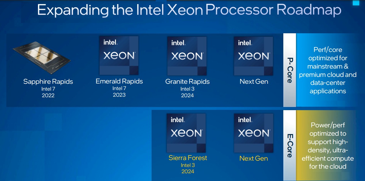
A little more than a year ago, this was the official public Intel Xeon SP roadmap:
The current “Sapphire Rapids” Xeon SP, the fourth generation in the Xeon “Scalable Processor” lineup, was etched using a refined 10 nanometer SuperFIN process, which the company renamed Intel 7, presumably because some of the attributes of the process were akin to the 7 nanometer processes from rivals Taiwan Semiconductor Manufacturing Co and Samsung Electronics. (No other foundries on Earth are offering 7 nanometer and smaller processes in volume production on server chips. You got three choices, although China’s Semiconductor Manufacturing International Corp (SMIC) says it reached 7 nanometers last August. For volume production, and in the wake of export controls on chip making gear, SMIC is focusing on its mature 28 nanometer processes and presumably is ramping its 14 nanometer processes even further.
The “Ice Lake” Xeon SP v3 got Intel out of the 14 nanometer box it was stuck in since the “Broadwell” Xeon E5 v4 processors in Q1 2016, all the way through the “Skylake” Xeon SP v1 in Q3 2017, the “Cascade Lake” Xeon SP v2 in Q2 2019 and its kicker the “Cascade Lake-R” Xeon SP v2 in Q1 2020. Sapphire Rapids was etched with that refined 10 nanometer SuperFIN process the chip maker renamed Intel 7. In late 2021, as far we knew and surmised from the rumor mills and chattering, Sapphire Rapids Xeon SP v3 chips were expected to be launched in Q2 2022, but that launch did not come until Q1 2023, although Intel did start shipping them to hyperscalers and cloud builders in the summer of 2022. Intel had announced a delay in the Intel 7 process way back in July 2020 that impacted Sapphire Rapids, and at that time, Intel was already six years late on 10 nanometer processes for Xeon server chips. And Intel continued to make lots of money because it could supply a hell of a lot more chips than TSMC could for AMD. What we call a supply win around The Next Platform. In any event, Sapphire Rapids was officially delayed in June 2021 to a Q1 2022 launch to give partners more time to validate the platform, with production expected to ramp in Q2 2022, but the launch didn’t happen until January 2023, as we said.
There are often delays with server CPU launches, official and behind the scenes, so no one can say it will never happen again. But it looks like Intel is going to do everything in its power to not only have it never happen again, but to move up process use and/or product launches to try to close the gap with AMD and the Arm collective.
This has happened once already, back in February 2022, and it just happened again this week.
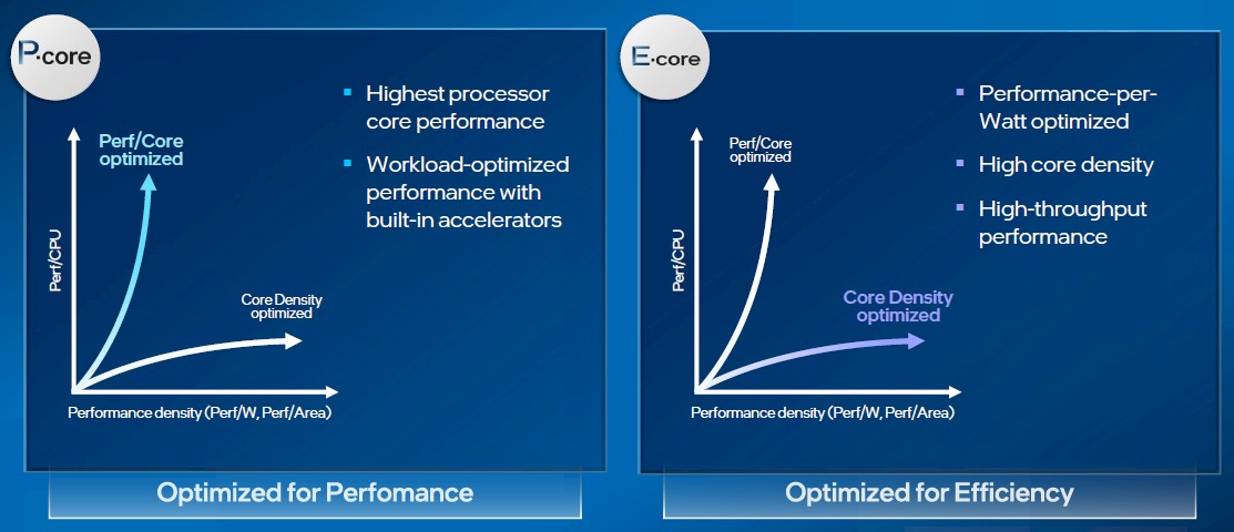
Last February, as we expected given AMD’s broadening of its product line by having standard parts and those with skinnier and more numerous cores – the “Genoa” Epyc 9004 is the standard part scaling to 96 cores, and the “Bergamo” chip will give something up or eat up more space to deliver 128 cores with better power efficiency – Intel admitted that it would deliver Xeon processors with its trimmed-down E-cores instead of the full-blown P-cores that are standard in the Xeon SP line.
At that time, Intel also admitted there was indeed a kicker to Sapphire Rapids that was socket compatible in the same “Eagle Stream” platform, which we know as “Emerald Rapids,” using a refined Intel 7 process and perhaps boosting maximum core count from 60 to the maximum of 64 as yields on that Intel 7 process improved.
“We have silicon on it today,” Singhal tells The Next Platform. “It’s going well, in terms of both functional validation as well as power and performance characterization. We see it very much meeting our expectations.” There are some minor microarchitecture tweaks, but nothing major, according to Singhal.
The Emerald Rapids Xeon SP v5 CPUs are slated for a Q4 2023 launch, and we think will largely replace mainstream Sapphire Rapids chips with the MCC tiles and up to 34 cores. Intel has not committed publicly to making an XCC version of Emerald Rapids that supports HBM memory, as it did with Sapphire Rapids, and Singhal was mum on the subject.
Importantly, Intel also said that “Granite Rapids,” a Xeon XP server CPU using P-cores in a new socket with a new “Mountain Stream” platform wrapped around it, would be shifting from the Intel 4 process – a super-refined 7 nanometer process that also added extreme ultraviolet, or EUV, wavelengths of light in its lithography – to a second generation of EUV called Intel 3, which is based on 5 nanometer geometries. This process was not expected to be used until 2025 in the “Diamond Rapids” Xeon SP v7 chip, which Intel has not discussed publicly. By pulling that process in by a year or so, Granite Rapids Xeon SP v6 can come out in 2024 and be a more competitive chip.
This same Intel 3 process was also slated for manufacturing the Sierra Forest E-core Xeon SP v6 chips, which were confirmed at the same time and which plug into the same “Birch Stream” and “Mountain Stream” platforms as the Granite Rapids chips. Intel 3 is a very big step improvement over Intel 7 – that is for sure.
With this week’s announcements, we learned a little more about Sierra Forest. Singhal told us it would have 144 cores in a single package and that the E-core would strip out the AVX-512 vector math units, the AMX matrix math units, and the HyperThreading implementation of simultaneous multithreading, which provides two virtual threads for each core. This is akin to what Ampere Computing has done with its minimalist (yet powerful) Arm cores, and what we think AMD will also do with Bergamo Epycs.
According to Spelman, Sierra Forest has “excellent silicon health” and after getting the first ones back from the Intel foundry, the silicon was powered on and operating systems were booted on them in under 18 hours. (We have no idea if that is impressive, but we are sure we were supposed to take away that impression.) Here is a demo screen showing all 144 cores on Sierra Forest booted up:
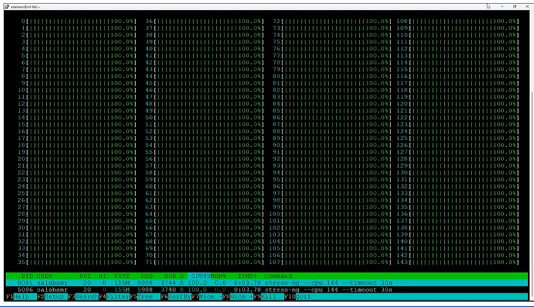
Looks very 1980s. . . .
The exciting bit is that Sierra Forest is blazing the trail for the Intel 3 process (Intel 4 is being left for certain PC CPUs at this point), and it will blaze the trail for Granite Rapids, which will “follow close on the heels” of Sierra Forest in Q3 2024.
Here is the latest Xeon roadmap:
Be careful there, because this one splits the P-core chips on the left side and the E-core chips on the right side, and it accidentally might lead you to believe that Sierra Forest comes after Granite Rapids. It is the other way around.
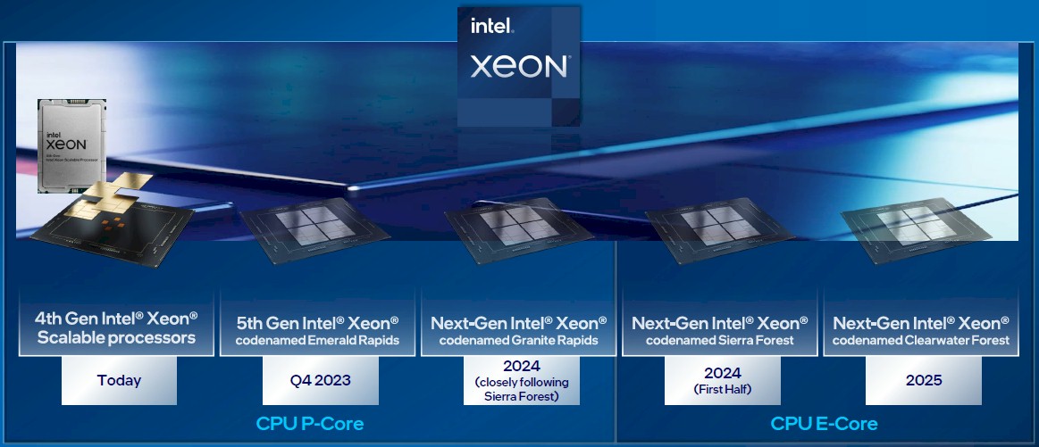
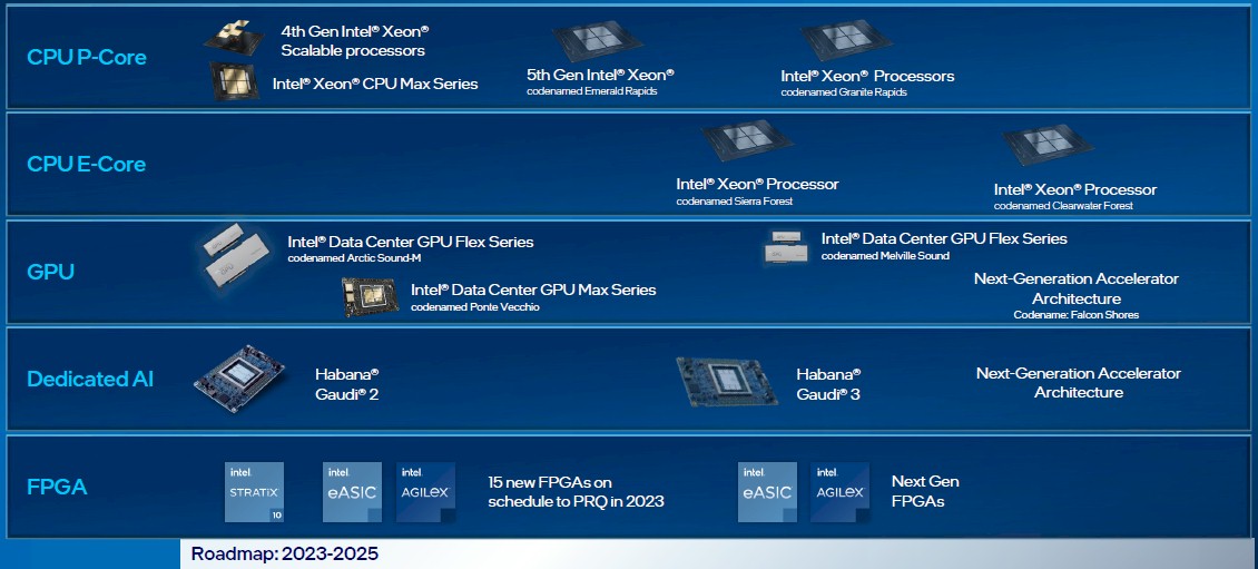
This broader Intel compute engine roadmap is perhaps better:
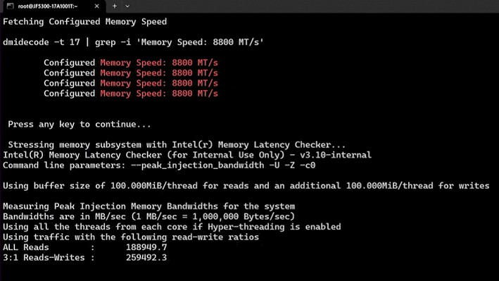
The one thing that Intel did divulge about Granite Rapids, aside from it coming to market a quarter earlier than the last time Intel put out a roadmap, is that the chip will make use of a special kind of DDR5 memory called Multiplexer Combined Rank (MCR) memory, which Intel developed in conjunction with memory maker SK Hynix. The MCR variant of DDR5 memory has a buffer chip that front ends a dual-rank memory module, allowing it to double its bandwidth out to the CPU. The MCR-DRAM memory shown in a test by Spelman ran at an effective 8.8 GT/sec (two ranks each running at 4.4 GHz is our guess), and on a two-socket server delivered 1.5 TB/sec of aggregate peak memory bandwidth. That is 1.8X better than what you can get on a two-socket Sapphire Rapids server right now, says Singhal.
Here is the memory stress test that Spelman showed:
On both of the roadmaps above, you will see that Intel has given a name to the kicker to Sierra Forrest but it still has not admitted there is a Diamond Rapids chip at all, much less one coming with this kicker, called “Clearwater Forest,” that is coming in 2025 and very significantly will be using the Intel 18A process, not the Intel 20A process originally expected. This is the fifth chip making process in four years that Gelsinger promised would be delivered. We had expected it to come first on Diamond Rapids, not Clearwater Forest. But maybe the cloud builders and hyperscalers want 18A to make its debut on the many core versions of the Xeon SPs. That is certainly what is happening.
The Xeon SP launch cadence, which is obvious in the chart above, certainly implies there will be a Xeon SP v7 chip sometime in 2025, which we are still calling Diamond Rapids.
The Gaudi 3 matrix compute engine for AI training and inference is “taping-in” right now – meaning starting the final processes that lead to the tape-out phase that comes before lithography masks are made for actual etching of a chip – and the Gaudi 3 chip is expected sometime in 2024. The Gaudi 2 chip was launched in May 2022, and a two-year cadence puts the Gaudi 4 sometime in 2026. But to our eye, it looks like Intel wants Gaudi 4 sometime in 2025, which is also when the “Falcon Shores” hybrid CPU-GPU package is expected to come to market.
That Intel GPU roadmap was already recently revised, with “Rialto Bridge” being canceled for next year, but we think Intel is missing opportunities without Rialto Bridge and Emerald Rapids with HBM. But, with a need to cut costs and hit targets, Intel has to trim back some of its ambitions so it can execute perfectly. But is it still going to be making datacenter GPUs.

The Bellwethers Of Enterprise IT Spending Fare Reasonably Well
If you want to figure out what is going on with spending on the corporate datacenters of the world, a good place to start is to examine the financial results of Hewlett Packard Enterprise and Dell Technologies, which are still the two largest original equipment makers for servers in the …
TSMC Makes The Best Of A Tough Chip Situation
If you had to sum up the second half of 2022 and the first half of 2023 from the perspective of the semiconductor industry, it would be that we made too many CPUs for PCs, smartphones, and servers and we didn’t make enough GPUs for the datacenter. Or rather, Taiwan …
Oracle Still Hanging In There With Exadata Engineered Systems
It may not seem like it, but Oracle is still in the high-end server business, at least when it comes to big machines running its eponymous relational database. In fact, the company has launched a new generation of Exadata database servers, and the architecture of these machines shows what is …
Aaahhh, the smell of skunkworks, the perfume of focused engineering, 18-hour shifts without food, bathroom breaks, sleep, or showers … but somebody please tell user salabamr to stop hogging the Sierra Forest with his/her 144 x 100% utilization job!
Hey, Intel. Change the name from e-Cores to A-Cores (anemic cores).
Or Atom cores!
With new Architecture, number of cores more leading to new AI machine. A demonstration gives more information regarding things.
Xeon e-Cores will steal a lot of oxygen (money) from server ARM demand.
Well, it will certainly give pause to the market. A lot depends on the integer and floating point performance of the cores. Intel will have integer performance, but without AMX and without AVX-512, what is the floating point gonna look like? Ampere Altra has some decent FP, so does Graviton3. We shall see about Bergamo and Sierra Forest. And and and, it all depends on price. If this is Atom, The Sequel, and the E-core chips are — pardon me — cheap as chips, yes, I agree, Intel could be a bigtime spoiler. But no one will make much money off these chips — not compared to P-core type devices.
“…without Rialto Bridge and Emerald Rapids with HBM.”
You said Intel didn’t comment on EMR-MAX; but now you seem to be announcing there will not be an EMR-MAX.
Well, they didn’t comment on it, so I am getting hints to not expect HBM with Emerald Rapids because I don’t think EMR will have an XCC variant. Hence no HBM controllers, and hence only a monolithic chip. And with Granite, Intel might be thinking the MCR memory is good enough until there is a hybrid Falcon Shores, and as far as I can tell, the first Falcon Shores will probably not be a hybrid P-core + GPU setup, but all GPU. In effect, it is a multi-chiplet discrete GPU until the market proves it wants CPU-GPUs in tight ratios.
Intel said Emerald Rapids will have more cores than Sapphire Rapids so that means Intel will be making an XCC version of Emerald Rapids. There seems to be a design flaw in the implementation of HBM on Sapphire Rapids. The four stacks of HBM2e used on the Xeon Max version of Sapphire Rapids should be capable of 1.6 TBytes/sec but the Xeon Max version of Sapphire Rapids provides ~1 TByte/sec. Perhaps this will be fixed on the Xeon Max version of Emerald Rapids. For Granite Rapids, four stacks of HBM3 is capable of 2.6 TBytes/sec, which is about 3.1x more than 12 channels of Multiplexer Combined Rank (MCR) DRAM DIMMs running at 8.8 GT/sec. I therefore expect to see a Xeon Max version of Granite Rapids with HBM3.
From your fingertips to Pat’s ears….