
System architects are often impatient about the future, especially when they can see something good coming down the pike. And thus, we can expect a certain amount of healthy and excited frustration when it comes to the Compute Express Link, or CXL, interconnect created by Intel, which with the absorption of Gen-Z technology from Hewlett Packard Enterprise and now OpenCAPI technology from IBM will become the standard for memory fabrics across compute engines for the foreseeable future.
The CXL 2.0 specification, which brings memory pooling across the PCI-Express 5.0 peripheral interconnect, will soon available on CPU engines. Which is great. But all eyes are already turning to the just-released CXL 3.0 specification, which rides atop the PCI-Express 6.0 interconnect coming in 2023 with 2X the bandwidth, and people are already contemplating what another 2X of bandwidth might offer with CXL 4.0 atop PCI-Express 7.0 coming in 2025.
In a way, we expect for CXL to follow the path blazed by IBM’s “Bluelink” OpenCAPI interconnect. Big Blue used the Bluelink interconnect in the “Cumulus” and “Nimbus” Power9 processors to provide NUMA interconnects across multiple processors, to run the NVLink protocol from Nvidia to provide memory coherence across the Power9 CPU and the Nvidia “Volta” V100 GPU accelerators, and to provide more generic memory coherent links to other kinds of accelerators through OpenCAPI ports. But the path that OpenCAPI and CXL will not be exactly the same, obviously. OpenCAPI is kaput and CXL is the standard for memory coherence in the datacenter.
IBM put faster OpenCAPI ports on the “Cirrus” Power10 processors, and they are used to provide those NUMA links as with the Power9 chips as well as a new OpenCAPI Memory Interface that uses the Bluelink SerDes as a memory controller, which runs a bit slower than a DDR4 or DDR5 controller but which takes up a lot less chip real estate and burns less power – and has the virtue of being exactly like the other I/O in the chip. In theory, IBM could have supported the CXL and NVLink protocols running atop its OpenCAPI interconnect on Power10, but there are some sour grapes there with Nvidia that we don’t understand – it seems foolish not to offer memory coherence with Nvidia’s current “Ampere” A100 and impending “Hopper” H100 GPUs. There may be an impedance mismatch between IBM and Nvidia in regards to signaling rates and lane counts between OpenCAPI and NVLink. IBM has PCI-Express 5.0 controllers on its Power10 chips – these are unique controllers and are not the Bluelink SerDes – and therefore could have supported the CXL coherence protocol, but as far as we know, Big Blue has chosen not to do that, either.
Given that we think CXL is the way a lot of GPU accelerators and their memories will link to CPUs in the future, this strategy by IBM seems odd. We are therefore nudging IBM to do a Power10+ processor with support for CXL 2.0 and NVLink 3.0 coherent links as well as with higher core counts and maybe higher clock speeds, perhaps in a year or a year and a half from now. There is no reason IBM cannot get some of the AI and HPC budget given the substantial advantages of its OpenCAPI memory, which is driving 818 GB/sec of memory bandwidth out of a dual chip module with 24 cores. We also expect for future datacenter GPU compute engines from Nvidia will support CXL in some fashion, but exactly how it will sit side-by-side with or merge with NVLink is unclear.
It is also unclear how the Gen-Z intellectual property donated to the CXL Consortium by HPE back in November 2021 and the OpenCAPI intellectual property donated to the organization steering CXL by IBM last week will be used to forge a CXL 4.0 standard, but these two system vendors are offering up what they have to help the CXL effort along. For which they should be commended. That said, we think both Gen-Z and OpenCAPI were way ahead of CXL and could have easily been tapped as in-node and inter-node memory and accelerator fabrics in their own right. HPE had a very elegant set of memory fabric switches and optical transceivers already designed, and IBM is the only CPU provider that offered CPU-GPU coherence across Nvidia GPUs and the ability to hook memory inside the box or across boxes over its OpenCAPI Memory Interface riding atop the Bluelink SerDes. (AMD is offering CPU-GPU coherence across its custom “Trento” Epyc 7003 series processors and its “Aldebaran” Instinct MI250X GPU accelerators in the “Frontier” exascale supercomputer at Oak Ridge National Laboratories.)
We are convinced that the Gen-Z and OpenCAPI technology will help make CXL better, and improve the kinds and varieties of coherence that are offered. CXL initially offered a kind of asymmetrical coherence, where CPUs can read and write to remote memories in accelerators as if they are local but using the PCI-Express bus instead of a proprietary NUMA interconnect – that is a vast oversimplification – rather than having full cache coherence across the CPUs and accelerators, which has a lot of overhead and which would have an impedance mismatch of its own because PCI-Express was, in days gone by, slower than a NUMA interconnect.
But as we have pointed out before, with PCI-Express doubling its speed every two years or so and latencies holding steady as that bandwidth jumps, we think there is a good chance that CXL will emerge as a kind of universal NUMA interconnect and memory controller, much as IBM has done with OpenCAPI, and Intel has suggested this for both CXL memory and CXL NUMA and Marvell certainly thinks that way about CXL memory as well. And that is why with CXL 3.0, the protocol is offering what is called “enhanced coherency,” which is another way of saying that it is precisely the kind of full coherency between devices that, for example, Nvidia offers across clusters of GPUs on an NVSwitch network or IBM offered between Power9 CPUs and Nvidia Volta GPUs. The kind of full coherency that Intel did not want to do in the beginning. What this means is that devices supporting the CXL.memory sub-protocol can access each other’s memory directly, not asymmetrically, across a CXL switch or a direct point-to-point network.
There is no reason why CXL cannot be the foundation of a memory area network as IBM has created with its “memory inception” implementation of OpenCAPI memory on the Power10 chip, either. As Intel and Marvell have shown in their conceptual presentations, the palette of chippery and interconnects is wide open with a standard like CXL, and improving it across many vectors is important. The industry let Intel win this one, and we will be better off in the long run because of it. Intel has largely let go of CXL and now all kinds of outside innovation can be brought to bear.
Ditto for the Universal Chiplet Interconnect Express being promoted by Intel as a standard for linking chiplets inside of compute engine sockets. Basically, we will live in a world where PCI-Express running UCI-Express connects chiplets inside of a socket, PCI-Express running CXL connects sockets and chips within a node (which is becoming increasingly ephemeral), and PCI-Express switch fabrics spanning a few racks or maybe even a row someday use CXL to link CPUs, accelerators, memory, and flash all together into disaggregated and composable virtual hardware servers.
For now, what is on the immediate horizon is CXL 3.0 running atop the PCI-Express 6.0 transport, and here is how CXL 3.0 is stacking up against the prior CXL 1.0/1.1 release and the current CXL 2.0 release on top of PCI-Express 5.0 transports:
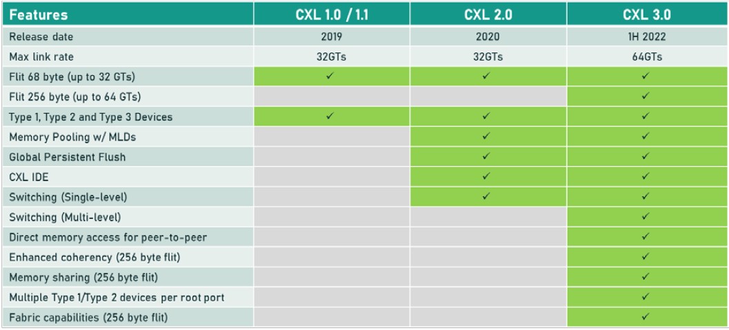
When the CXL protocol is running in I/O mode – what is called CXL.io – it is essentially just the same as the PCI-Express peripheral protocol for I/O devices. The CXL.cache and CXL.memory protocols add caching and memory addressing atop the PCI-Express transport, and run at about half the latency of the PCI-Express protocol. To put some numbers on this, as we did back in September 2021 when talking to Intel, the CXL protocol specification requires that a snoop response on a snoop command when a cache line is missed has to be under 50 nanoseconds, pin to pin, and for memory reads, pin to pin, latency has to be under 80 nanoseconds. By contrast, a local DDR4 memory access one a CPU socket is around 80 nanoseconds, and a NUMA access to far memory in an adjacent CPU socket is around 135 nanoseconds in a typical X86 server.
With the CXL 3.0 protocol running atop the PCI-Express 6.0 transport, the bandwidth is being doubled on all three types of drivers without any increase in latency. That bandwidth increase, to 256 GB/sec across x16 lanes (including both directions) is thanks to the 256 byte flow control unit, or flit, fixed packet size (which is larger than the 64 byte packet used in the PCI-Express 5.0 transport) and the PAM-4 pulsed amplitude modulation encoding that doubles up the bits per signal on the PCI-Express transport. The PCI-Express protocol uses a combination of cyclic redundancy check (CRC) and three-way forward error correction (FEC) algorithms to protect the data being transported across the wire, which is a better method than was employed with prior PCI-Express protocols and hence why PCI-Express 6.0 and therefore CXL 3.0 will have much better performance for memory devices.
The CXL 3.0 protocol does have a low latency CRC algorithm that breaks the 256 B flits into 128 B half flits and does its CRC check and transmissions on these subflits, which can reduce latencies in transmissions by somewhere between 2 nanosecond and 5 nanoseconds.
The neat new thing coming with CXL 3.0 is memory sharing, and this is distinct from the memory pooling that was available with CXL 2.0. Here is what memory pooling looks like:
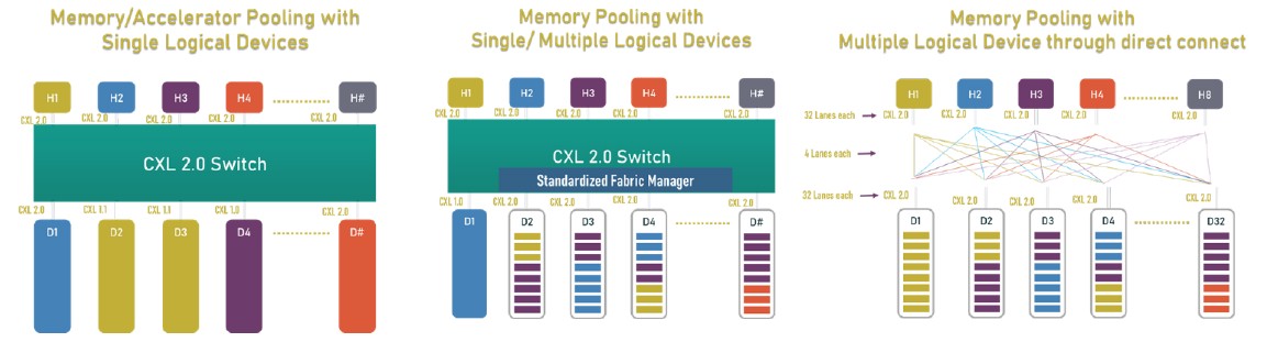
With memory pooling, you put a glorified PCI-Express switch that speaks CXL between hosts with CPUs and enclosures with accelerators with their own memories or just blocks of raw memory – with or without a fabric manager – and you allocate the accelerators (and their memory) or the memory capacity to the hosts as needed. As the diagram above shows on the right, you can do a point to point interconnect between all hosts and all accelerators or memory devices without a switch, too, if you want to hard code a PCI-Express topology for them to link on.
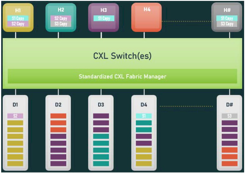
With CXL 3.0 memory sharing, memory out on a device can be literally shared simultaneously with multiple hosts at the same time. This chart below shows the combination of device shared memory and coherent copies of shared regions enabled by CXL 3.0:
System and cluster designers will be able to mix and match memory pooling and memory sharing techniques with CXL 3.0. CXL 3.0 will allow for multiple layers of switches, too, which was not possible with CXL 2.0, and therefore you can imagine PCI-Express networks with various topologies and layers being able to lash together all kinds of devices and memories into switch fabrics. Spine/leaf networks common among hyperscalers and cloud builders are possible, including devices that just share their cache, devices that just share their memory, and devices that share their cache and memory. (That is Type 1, Type 3, and Type 2 in the CXL device nomenclature.)
The CXL fabric is what will be truly useful and what is enabled in the 3.0 specification. With a fabric, a you get a software-defined, dynamic network of CXL-enabled devices instead of a static network set up with a specific topology linking specific CXL devices. Here is a simple example of a non-tree topology implemented in a fabric that was not possible with CXL 2.0:
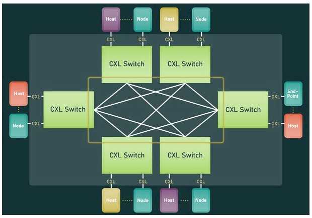
And here is the neat bit. The CXL 3.0 fabric can stretch to 4,096 CXL devices. Now, ask yourself this: How many of the big iron NUMA systems and HPC or AI supercomputers in the world have more than 4,096 devices? Not as many as you think. And so, as we have been saying for years now, for a certain class of clustered systems, whether the nodes are loosely or tightly coupled at their memories, a PCI-Express fabric running CXL is just about all they are going to need for networking. Ethernet or InfiniBand will just be used to talk to the outside world. We would expect to see flash devices front-ended by DRAM as a fast cache as the hardware under storage clusters, too. (Optane 3D XPoint persistent memory is no longer an option. But there is always hope for some form of PCM memory or another form of ReRAM. Don’t hold your breath, though.)
As we sit here mulling all of this over, we can’t help thinking about how memory sharing might simplify the programming of HPC and AI applications, especially if there is enough compute in the shared memory to do some collective operations on data as it is processed. There are all kinds of interesting possibilities. . . .
Anyway, making CXL fabrics is going to be interesting, and it will be the heart of many system architectures. The trick will be sharing the memory to drive down the effective cost of DRAM – research by Microsoft Azure showed that on its cloud, memory capacity utilization was only an average of about 40 percent, and half of the VMs running never touched more than half of the memory allocated to their hypervisors from the underlying hardware – to pay for the flexibility that comes through CXL switching and composability for devices with memory and devices as memory.
What we want, and what we have always wanted, was a memory-centric systems architecture that allows all kinds of compute engines to share data in memory as it is being manipulated and to move that data as little as possible. This is the road to higher energy efficiency in systems, at least in theory. Within a few years, we will get to test this all out in practice, and it is legitimately exciting. All we need now is PCI-Express 7.0 two years earlier and we can have some real fun.


Datacenter Is The New Unit Of Compute, Open Networking Is How To Automate It
Datacenters have evolved from physical servers, to virtualized systems, and now to composable infrastructure where resources such as storage and persistent memory are disaggregated from the server. At the same time, processing has evolved from running only on CPUs to accelerated computing running on GPUs, DPUs, or FPGAs to handle …
Why There’s Hard, Cold Cash For Soft, Disaggregated Routing
No matter if you are talking about compute or networking, there are two opposing forces that are constantly at interplay on a field of green money. The first force is the desire to implement as many specialized functions in transistors to accelerate the performance of those functions. The other force …
Intel Declares A Truce Before Bus Wars Flare Up
A system is more than its central processor, and perhaps at no time in history has this ever been true than right now. Except, perhaps, in the future spanning out beyond the next decade until CMOS technologies finally reach their limits. Looking ahead, all computing will be hybrid, using a …
The 4,096 device limit in CXL 3.0 may work for machines like Adastra (338 nodes x 1 EPYC + 4 MI250x per node = 1690 devices, plus some CXL memory) but LUMI, Frontier and Fugaku are bigger (near 160,000 for Fugaku) and so I hope that CXL 4.0 will increase this limit (20-bit addressing would be neat!). Still, the 256 Byte flits sound good for supporting 2,048-bit vectors in AVX and SVE, as that’s two 4×4 double-precision matrices (or more in SP) for FMA …
Note that each CXL 3.0 Fabric supports up to 4096 Devices, and each Root Port (RP) of a CPU may belong to a different CXL 3.0 Fabric. In other words, we are not limited to 4096 Devices in a “large” ensemble of CXL-connected platform/Fabric.
That makes perfect sense; thanks for the clarification!
In none of the descriptions and pictures is an independent central memory management unit or a hypervisor-like component or anything similar to be seen. This raises two questions: How is CXL memory allocation, addressing and protection done? More importantly, whether and, if so, how security is ensured in the case of non-cooperating or even malicious OS instances?
Intel’s CXL “won” because nearly every company other than perhaps Nvidia lacks the fortitude to develop and drive interconnect and fabric innovation without Intel. It really is that simple. IBM delivered a solid OpenCAPI implementation, but Power-based systems are a niche play, and again, without Intel, it stood zero chance of volume adoption. Gen-Z garnered some earlier proof-of-concept adopters, but strong product commitments never really materialized. It is now apparent that most of these companies were not backing Gen-Z because it was significantly more robust / capable than CXL or UCI Express, but solely as a way to push Intel (the volume processor leader) to open up enough of its proprietary coherency to attach accelerators and memory devices which is where the non-processor hardware industry makes money. Just compare the tables and figures in this article with those put forward several years ago by the Gen-Z Consortium to see how CXL 3.0 is just starting to approach what Gen-Z had fully specified and could scale from chip-to-chip to board-to-module to enclosure-to-enclosure with far less complexity. It is unfortunate that Intel’s NIH culture and walled garden leadership prevented it from joining the Gen-Z Consortium as the industry would already be delivering robust, scalable solutions.
The more interesting question now is will any of this really matter? Robust, composable infrastructure has been the promised nirvana of multiple industry efforts for decades. The industry promised InfiniBand would be the breakthrough technology to deliver a superior high-performance composable I/O fabric, but failed to be processor integrated and was reduced to being yet another low-latency messaging interconnect. Intel’s vaunted Advanced Switching (championed by Pat Gelsinger) was going to take the world by storm as it was built on top of PCI Express, but it too failed as even Intel would not integrate it into its processors. CXL advocates will say this time is different because everyone will integrate CXL into processors. However, processor-integration is critical only in a processor-centric world, and most who have studied data access will tell you that processing is best performed as close to where the data resides to deliver optimal performance / watt / dollar. With the ability to integrate intelligence into nearly any memory or storage module without modifying the underlying data devices with very little incremental cost, one has to really question whether specialized interconnects like CXL will ultimately matter beyond point-to-point solutions. Lot of money and resources will be spent finding out, but if history is any guide, it is a long shot at best. Anyway, just something to think about.
Ouch. Good points, though. Hope is cheap, I know, and execution is expensive, I know. But maybe this time really will be different. Sometimes, it is.
I wonder if a device that combines 80GB or 128GB of HBM, with a fast processing unit, could be considered computational memory (these would be the A100 and MI250x)? The processor writes data to it, writes code to it, and then reads off the results from it. Maybe it requires too much power or is too small relative to expected conventional memory size to be considered computational memory (?). I wonder (and don’t know the answer to this) where the line is drawn between computational memory, and a “large” chunk of memory fronted by a processor within a larger computational system.
You are very funny.
But seriously, from the GPU’s point of view, the CPU is just an serial accelerator that handles some I/O housekeeping tasks and has a huge block of cheap and slow memory that acts more or less like an L4 cache for its HBM…..
Thank you very much! I’m here all weak (he-he-he)!
Wonder what the blast radius is for an error in the interconnect. How much is affected if something goes bad? I haven’t seen this discussed anywhere, and it’s not a small consideration.
That’s a fair point. I suppose it is as big as the host or an individual PCI-Express switch, which is probably why there will be redundancies in the different PCI-Express switch layers, just as there are for other kinds of leaf/spine networks.
So you could have a whole big block of remote memory suddenly taken off line due to a PCIe failure. Ouch!
IIRC, PCI Express / CXL / CCIX do not support transparent end-to-end transaction retransmission, which means that if a link or switch fails, then everything below will be inaccessible and a good implementation will trigger containment. This is really no worse than DDR in one sense, but keep in mind that DDR DIMMs sit right next to the processor on the same motherboard and are not customer accessible. This is not the case in composable solutions where I/O, memory, and storage modules are customer accessible and are typically provisioned in an independent cable-attached enclosure which contain independent power, cooling, and management domains.
OpenCAPI was limited to point-to-point topologies within a single enclosure, so an intelligent implementation with multiple links could support end-to-end transaction retransmission. Gen-Z supported transparent link and end-to-end transaction retransmission, so multi-link components can transparently survive link and switch failure (surprise cable disconnects occur at a much higher rate than you might realize). It is unclear if CXL can or will adapt any of Gen-Z’s resiliency capabilities as the volume processor companies have always opposed such stating that these are “high-end” features, and such capabilities are best built into the architecture core from the start (retrofits rarely work and even when they do, they come with a lot of caveats). However, I suspect many customers will be reluctant to deploy composable infrastructures en masse without such features. Also, keep in mind that cloud providers build solutions where they assume everything can and will fail, hence, don’t they care about such resiliency and are highly unlikely to deploy composable infrastructure as it does not fit their cost and operating / execution models.
I recall comments that cxl was intended to be a simpler solution, easy to implement in the GPUs or other accelerators. I wonder what are the solutions to maintain that simplicity, while the added opencapi and genz functions of cxl 3.0 are being globbed on.
Is it effectively all just a free-for-all after taking control of the pcie lanes?
That seems pretty accurate….hopefully in a good way.