
What is the most expensive component that hyperscalers and cloud builders put into their X86 servers? It is the GPU accelerator, correct. So let’s ask this question another way: What is the most expensive component in the more generic, non-accelerated servers that comprise the majority of their server fleets? Main memory, correct again.
If you do the math on what things costs over time, about a decade ago the CPU used to comprise about half of the basic server cost in the datacenter for infrastructure workloads; HPC systems were a little more intense on cores and a little less intense on memory. Memory was about 15 percent of the system cost, the motherboard was about 10 percent, and local storage (which was a disk drive) was somewhere between 5 percent and 10 percent, depending on how fat or fast you wanted that disk. The power supply, network interfaces, and chassis made up the rest, and in a lot of cases the network interface was on the motherboard already, so that cost was bundled in already except in cases where companies wanted a faster Ethernet or InfiniBand interface.
Over time, flash memory was added to systems, main memory costs for servers spiked through the roof (but have some down some relative to the price of other components), and competition returned to X86 CPUs with the re-entry of AMD. And so the relative slice sizes in the server cost pie for generic servers widened and shrank here and there. Depending on the configuration, the CPU and the main memory comprise about a third of the cost of the system each, and these days, memory is usually more expensive than the CPU. With the hyperscalers and cloud builders, memory is definitely is the most expensive item because the competition is more intense on the X86 CPUs, driving the cost down. Server main memory is in relative short supply – and intentionally so as Micron Technology and Samsung and SK Hynix Flash and disk together are around 10 percent of the cost, the motherboard is around 5 percent of the cost, and the rest is the chassis and other peripherals.
An interesting aside: According to Intel, the CPU still represents about 32 percent of the IT equipment power budget, with memory only burning 14 percent, peripheral costs around 20 percent, the motherboard around 10 percent, and disk drives 5 percent. (Flash is in the peripheral part of the power budget pie, we presume.) The IT equipment – compute, storage, and networking – eats a little less than half of the power, and power conditioning, lighting, security systems, and other aspects of the datacenter facility eat up a little more than half, and that gives a rather pathetic power usage effectiveness of 1.8, more or less. The typical hyperscale and cloud builder datacenter has a PUE of around a 1.2.
Suffice it to say, memory is a big cost factor, and with plenty of applications being constrained on memory bandwidth and memory capacity, disaggregating main memory from the CPU, and indeed any compute engine, is part of the composable datacenter that we write about a lot here at The Next Platform. And the reason is simple: We want the I/O coming off the chips to be configurable, too, and that means, in the long run, converging the memory controllers and PCI-Express controllers, or coming up with a generic transport and controller that can speak either I/O or memory semantics depending on what is plugged into a port. IBM has done the latter with its OpenCAPI Memory Interface on the Power10 processor, but we think over time Intel and others will do the former with the CXL protocol running atop the PCI-Express transport.
Chip maker Marvell, which no longer is trying to sell its ThunderX family of Arm server CPUs into the datacenter, nonetheless wants to get in on the CXL memory game. And to that end, back in early May it acquired a startup called Tanzanite Silicon Solutions for its Smart Logic Interface Connector, which is a CXL bridge between CPUs and memory that is going to help smash the server and stitch it back together again in a composable way – something we have been talking about since before The Next Platform was established. Tanzanite was founded in 2020 and demonstrated the first CXL memory pooling for servers last year using FPGAs as it is putting the finishing touches on its SLIC chip.
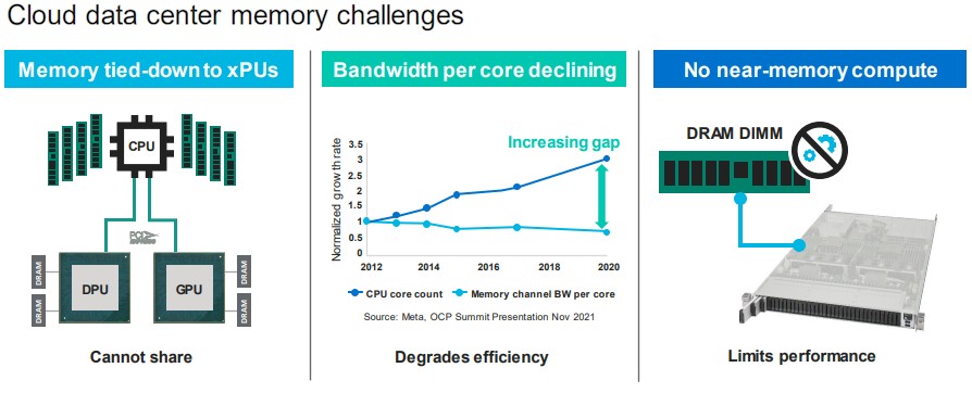 “Today, memory has to be attached to a CPU, a GPU, a DPU, whatever through a memory controller,” Thad Omura, vice president of the flash business unit at Marvell, tells The Next Platform. “And there are two problems with this. One, very expensive memory ends up either being underutilized or, worse yet, unused. And in some cases, there is more underutilization than just the memory. If you need more memory for big workloads, sometimes you add another CPU to the system to boost the memory capacity and bandwidth, and that CPU can be underutilized, too. And that is really the second problem: This infrastructure cannot scale. You cannot add more memory to the system without adding more CPUs. So the question is this: How do you get the memory to be shareable and scalable?”
As Omura points out in the chart above, another issue is that core counts on CPUs are expanding faster than memory bandwidth, so there is a widening gap between the performance of the cores and the DIMMs that feed them, as the Meta Platforms data above shows. And finally, aside from some science projects, there is no way to aggregate memory and move compute closer to it so it can be processed in place, which is limiting the overall performance of systems. Gen Z from Hewlett Packard Enterprise, OpenCAPI from IBM, and CCIX from Xilinx and the Arm collective were all contenders to be a converged memory and I/O transport, but clearly Intel’s CXL has emerged as the standard that everyone is going to rally behind in the long run.
“CXL is gaining a lot of traction, and are working with basically all the major hyperscalers on their architectures, helping them figure out how they are going to deploy this technology,” says Omura. Hence, the Tanzanite acquisition, the value of which was not disclosed, which closed at the end of May.
With the SLIC chip, Marvell will be able to help the industry create standard DIMM form factors with CXL expander controllers as well as fatter and taller expanded memory modules that are larger than DIMM form factors. (IBM has done the latter with several generations of its Power Systems servers and their homegrown “Centaur”: buffered memory controllers.)
The first thing that CXL memory is going to do its open up the memory bandwidth over both the DRAM and PCI-Express controllers on modern processors, says Omura. And we agree.
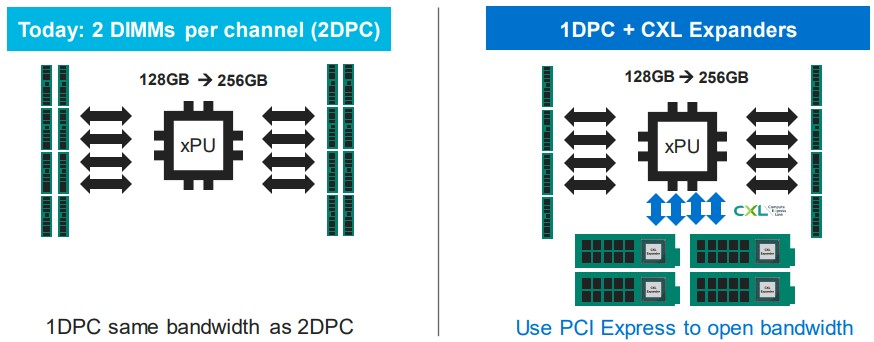
If you have a system today and you have a set bandwidth across its memory slots, you can increase capacity by adding two DIMMs per memory channel, but then each DIMM gets half the memory bandwidth. But with the addition of CXL memory DIMMs to the system using the SLIC chip, you can use a significant portion of the PCI-Express bus to add more memory channels to the system. Admittedly, the bandwidth coming out of PCI-Express 5.0 slots is not as high and the latency is not as low as with the DRAM controllers on the chip, but it works. And at some point, when PCI-Express 6.0 is out, there may not be a need for DDR5 or DDR6 memory controllers in certain classes of processors, and DDR controllers may turn into exotic parts much as HBM stacked memory is exotic and only for special use cases. The hope to CXL memory over PCI-Express 5.0 and 6.0 will not be much worse (if at all) than going through the NUMA links to an adjacent socket in a multi-socket system, and it may be even less of a hassle once CXL ports literally are the main memory ports on systems and DDR and HBM are the specialized, exotic memory that is only used when necessary. At least that’s what we think might happen.
The CXL memory expansion is just the first stage in this evolution. It won’t be long before CXL chips like Marvell’s SLIC will be used to create shared memory pools across diverse – and often incompatible –compute engines, and even further down the road, we can expect for there to be CXL switching infrastructure that creates a composable fabric between different types of memory devices and different kinds of compute engines. Like this:

In the full vision that Marvell has, sometimes there will be some local memory on XPUs – the X is a variable for designating CPU, GPU, DPU, and so on – and a CXL ink over PCI-Express will hook out to a memory module that has integrated compute on it for doing specialized functions – and you can bet that Marvell wants to use its custom processor design team to help hyperscalers, cloud builders, and anyone else who has reasonable volumes put compute on memory and link it to XPUs. Marvell is also obviously keen on using the CXL controllers it is getting through the Tanzanite acquisition to create SmartNICs and DPUs that have native CXL capabilities and composability in their own right.
And then, some years hence, as we have talked about many times, we will get true composability within datacenter racks, and not just for GPUs and flash working over PCI-Express. But across compute, memory, and storage of all kinds.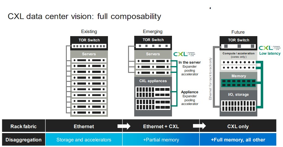
Marvell already has the compute (Octeon NPUs and custom ThunderX3 processors if you want them), DPUs and SmartNICs, electro-optics, re-timers, and SSD controllers needed in datacenter server and rack architectures, and now Tanzanite gives it a way to supply CXL expanders, CXL fabric switches, and other chippery that together comprise what Omura says is a “multi-billion dollar” opportunity.
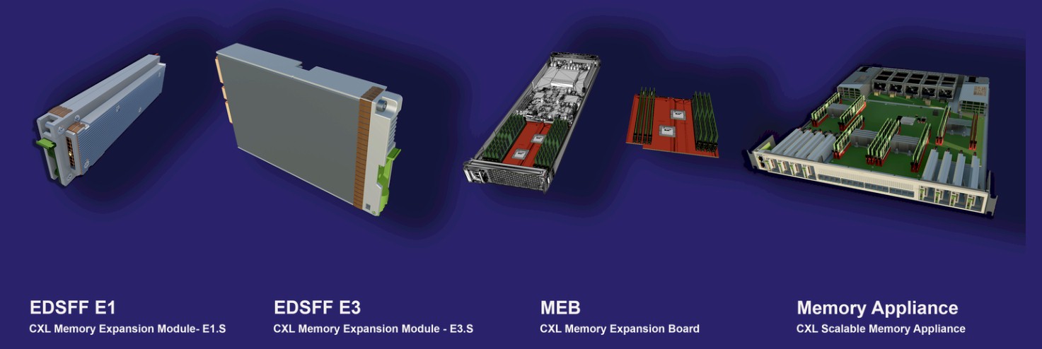
This is the opportunity that Tanzanite was created to chase, and here are the prototype use cases it had envisioned prior to the Marvell deal:
We think every one of these machines above will sell like hot cakes – provided the DRAM memory comes down in price a bit. Memory is still too expensive.

The Power Of Power10’s Memory Inception Clustering
Scanning through Power10’s detailed announcement material, I’ve seen a lot architecturally that intrigues an avid reader of The Next Platform like myself, but one item – one that IBM calls “Memory Inception” and IBM-based techie material calls enablement for a “memory cluster” – really caught my eye. It has the …
Marvell Throws Hat Into Intel’s Universal Chiplet Interconnect Ring
Marvell Technology is the latest chipmaker to join the emerging Universal Chiplet Interconnect Express (UCI-Express) consortium, which is working toward an open interconnect standard for chiplet architectures. The chipmaker joins several heavy hitters in the tech arena that have thrown their weight behind the project, including AMD, Arm, Qualcomm, and …
Photonics To Make Celestial HBM3 Memory Fabric
There is no shortage of silicon photonics technologies under development, and every few months it seems like another startup crops up promising massive bandwidth, over longer distances, while using less power than copper interconnects. Celestial AI is the latest contender to enter this space, having popped back up after a …
Could Apple use this SerDes-oriented CXL approach to provide random-access memory expansion for systems based on M1/M2 SOCs (i wonder)?
Why not? You just need PCI-Express and a decent implementation of CXL.
In the last picture, cxl only case: why not integrate io with tor switch? I.e cxl/pcie to ‘intelligent tor switch’
From what I understand, the defining property of big data is the need to move the program to where the data is stored rather than the data to where the program is running. Paradigms like map-reduce allow IO and memory bandwidth to scale linearly because the bottlenecked cost of copying code around is much less than transferring the data.
Having said this, I can see an advantage in composable IO and memory for large applications.
The consistent performance favoured by cloud providers may not be possible with transparently composed GPUs and RAM. Even so, since the timing-related side channels and latency would likely be less of a security problem than CPU threads, for example, such composability may still be useful in the cloud.
During the Meltdown and Spectre disclosures I thought the opposite idea of micro-sized single-tenant hardware with local everything might become popular. Full hardware isolation is not only good for consistent performance but security. However, then the silicon and energy shortage came along. Now it’s about utilisation and capacity.
Thanks for all the reporting and technical analysis. I always look forward to reading and thinking about new things.
I think this idea is much older than Google and MapReduce. Databases have been dealing with data locality across storage arrays and main memory for a long time, figuring out how to move SQL queries closer to the data and to parallelize the data access and the compute hitting it. Just like computing on the switch for collective operations makes sense — the switch is talking to all the endpoints in its domain, and can report up the switching tiers aggregated data to be scattered to the endpoints for further computation — maybe computing on the memory, at the DIMM level, for SQL operations (just an example) would mean less CPU-heavy joining in the main memories of the servers running the database. In a world where moving data is expensive, having some compute everywhere and some memory everywhere might be what happens.
How we might control all of this, heaven only knows.
How does this address the cost problem? It looks like a way to add more memory (and thus cost) to a server.
In my experience the increase in cost of memory is due to having to add 16 dimms to a server just to get the full bandwidth. That’s probably not true in other settings, where capacity is the premium attribute.
Just adding CXL memory to a server socket means two things. Now, to get a certain capacity, you can use skinnier and cheaper DIMMs if you need X capacity — and you get something like 1.7X the memory bandwidth. (The CXL memory is a little slower than native DIMMs, at least for now.) Also, if you need more memory for a certain price or more bandwidth, you don’t have to go to a machine with two or four or eight sockets.
Beyond that, once you have memory area network, (MAN?) you can have some memory local in each node and shared memory out on the MAN. And instead of having to put 256 GB or 512 GB or 1 TB on the node, maybe you put 128 GB on there and the rest is pulled off the MAN. Overall memory utilization rises across the cluster of machines sharing memory.
Or, better still, the server nodes have zero memory at all local and only pull from the MAN and zero flash local and pull from the FAN and zero disk local and pull from the SAN and zero CPU local and pull from the CAN. In other words, there is no server as we know it in the long run, Just trays of stuff. I doubt the utilization can be driven anywhere close to 100 percent for all components, of course, but the bet is that it will be higher than having everything statically defined on a motherboard.
So this works for big databases on big servers. (IBM, superdome) but that is probably not a large enough market to support the technology. What is the use for 1-2 socket servers running cloud/edge/hpc workloads? I guess it’s the MAN, and provisioning memory to the node as needed. Possibly integrated with k8s or a VM allocator. As I suspected, it doesn’t really fix the cost of the memory problem, it just fixes the cost of having to provision every node with memory that only some need. I just wonder if the cost goes down enough to make it worthwhile.
I think that making infrastructure stretch further and driving up utilization is the same thing as lowering its real costs.
As for making memory itself cheaper, I suppose there is a chance that we might be able to break out of the DIMM form factor at some point. But the memory cost is really down to the DRAM cost and the fact that memory makers get far more profit selling tiny pieces of memory for smartphones than they get from selling big hunks of it for servers, and that is why the price went up by 2X a few years ago. They like memory prices being high. They have come down some, and until we have a bust cycle where they are overprovisioning in their factories, it seems unlikely. And the memory DIMM makers might try to keep the server price high anyway.
Latency
Latency
Latency
How close can CXL come to 50ns latency? If it’s not close (say, within a factor of two compared to local RAM), then it’s just a new form of swap.
Can you get hard numbers from any vendors?
It’s a little bit more than a NUMA hop with PCI-Express 5.0. But it will be better as PCI-Express gets faster is the hope. Some data from Facebook:
https://www.nextplatform.com/2022/06/16/meta-platforms-hacks-cxl-memory-tier-into-linux/
IBM can do its OMI memory over Bluelink with an under 10 nanosecond add over its former memory controller. IBM’s implementation is quite good and shows the way.
While they’re not hard numbers, there’s also some comparison to RDMA here to show the level of improvement with CXL https://camel.kaist.ac.kr/public/camel-cxl-memory-pooling.pdf
Isn’t the bandwidth per core issue taken care of by things like 3DV cache both on CPU and GPU? I’ve read xDNA3 will is basically going with more Infinity Cache and narrower memory controllers and that some models will have 3D stacked Infinity Cache. At least in DC they’re also supposed to have coherent memory between CPU/GPU. IIRC AMD is also going to support CXL at some point, but isn’t it kind of a niche thing really considering those problems seem to already be kind of solved? Or am I completely missing something?
Great article and you mention Marvell Octeon NPUs?
Network Processor Units or is this a typo CPU/DPU?
Be good to explain the terminology.
Yes, Network Processing Unit. Apologies. Something for software-defined networking that predates the DPU, kinda.
CXL is a very exciting tech… I also just read an article involving “chiplet clouds” and that seems to be what AMD is working towards with 3d VCache… I expect that by Zen6 AMD will be using multiple stacks to keep even more data closer to the chiplet… From what I’ve seen these do sit between SRAM and HBM for complexity and bandwidth per module… Micron is working on 256GB DDR5 which will allow for up to 2TB RAM… It will be interesting to see how fast mobo makers add more CXL modules… Most servers need RAM more than PCIe devices so that means they can replace the PICe slots with CXL connectors…
AMD is already using them in EPYC servers and may be the first to make a chiplet-based DPU or FPGA…