

If the datacenter had been taken over by InfiniBand, as was originally intended back in the late 1990s, then PCI-Express peripheral buses and certainly PCI-Express switching – and maybe even Ethernet switching itself – would not have been necessary at all. But either thankfully or not, as you may see it, InfiniBand was not cheap enough to disrupt the long-held ways of building peripheral buses for systems and of using Ethernet for cross-system communication.
And so, the PCI-X bus and then the PCI-Express bus were developed and extended. You can see the evolution from the original PCI interconnect released in 1992 through the PCI-Express 6.0 specification expected to be ratified this year and appear in products maybe two years from now, in this story from August 2020. That story is a very CPU and server centric view of the PCI-Express bus. But there is another facet of PCI-Express that is becoming more relevant, and looks to be even more so with the PCI-Express 5.0 generation: PCI-Express switching. Microchip, a conglomerate that includes the Microsemi and PMC-Sierra chip businesses, is now sampling not only PCI-Express 5.0 switch chips, but also companion retimers that allow for PCI-Express 5.0 links to be extended beyond their fairly limited range on copper cabling.
We won’t say that PCI-Express switching was an accident, but if it was, it was a happy accident at least. It is a way to get lower latency interconnects between systems and peripherals without having to go through the InfiniBand and Ethernet stacks at all. And for an emerging set of vendors who sell tools for creating disaggregated and composable infrastructure, PCI-Express switching is the easiest, fastest, and preferred method.
Let’s explain the happy accident that created PCI-Express switching, which now does many of the things that were proposed with the original InfiniBand fabric way back when, before we get into the details of the new Switchtec PFX Gen 5 switch chips and their XpressConnect retimer chips.
Because of the relatively limited lane counts on modern CPUs and the desire to add lots of storage devices in storage arrays based on CPU architectures and then to add lots of GPUs and sometimes accelerators inside true compute servers, PCI-Express switches came into being. They were absolutely necessary when PCI-Express 4.0, whose specification should have been finalized in 2013 or so and appeared in products in maybe early 2015 or so, was held up and we were stuck at PCI-Express 3.0 speeds inside of systems and storage controllers. The only way to add more devices to machines during this time was to use PCI-Express switches between the fairly limited PCI-Express 3.0 (in terms of speed as well as lane count) controllers on the processors. And ironically, it was the storage vendors who pushed this approach and the server vendors who are really benefitting.
“At Gen 3.0, things started to expand the total addressable market for PCI-Express,” Ray Jang, product marketing manager for datacenter products at Microchip, recalls. “During this time, there were a number of startup companies who developed flash arrays that were all based on PCI-Express, and if you recall, a lot of them went bankrupt. They did not succeed and they just could not deliver a robust enough product. And tier one enterprise storage suppliers – the big names like EMC, Netapp, IBM, and so on, and they just couldn’t get to market with a product. And there was the genesis of us – meaning PMC-Sierra – getting into this business. We built SAS controllers and SAS expanders. And these customers came to us with a problem statement: I want to build what I had with SAS, but using PCI-Express.”
This was back when PLX Technology was the only supplier of PCI-Express switches and had not yet been bought by chip conglomerate Avago Technologies (which happened in June 2014), and less than a year later Avago bought switch ASIC maker and merchant switch pioneer Broadcom for $37 billion and took the Broadcom name.
The PCI-Express 3.0 switches “took the market by storm,” according to Jang, and they were a perfect fit for storage enclosures on adjacent shelves within a rack, using either copper or optical cables. From 2012 through 2013, the machine learning crazy powered by GPUs took off in academia and was soon followed among the hyperscalers and then the cloud builders at the same time that GPU acceleration was getting more firmly established in HPC simulation and modeling, and the same need arose: lash more GPUs to a server than the raw PCI-Express lanes on the CPUs could handle to boost the ratio of GPU compute to CPU compute. When PCI-Express 4.0 spec was finally done in 2017, the industry was eager to double up speeds from 8 GT/sec, which worked out to 32 GB/sec of bandwidth for a duplex x16 slot in a server to 16 GT/sec and 64 GB/sec. PCI-Express peripherals started coming out in late 2017 and as more and more CPUs supported PCI-Express 4.0 in 2019 and 2020, the need for PCI-Express 4.0 switching took off. By our reckoning, it would have been great if the switches from Microchip and Broadcom were out concurrent with the CPU support, and maybe with the PCI-Express 5.0 generation, we can get this all synched up so the system architecture is fully maxxed. One can hope.
Because the laws of physics are demanding, when you boost the bandwidth of a switch ASIC, it generally means cutting the length of the cables sending the signals by almost half. What this has meant is that as the industry has moved from PCI-Express 3.0 to 4.0 and then to 5.0, the cable lengths are getting shorter and shorter. With PCI-Express 3.0 switching, the bandwidth was low enough and the signal strong enough within a set power envelope so you could span three racks or so with copper cables. With PCI-Express 4.0 switches, the bandwidth doubled, but the cable lengths were cut. You could switch between CPUs and peripherals within an enclosure, but you needed retimers to boost the signal out to adjacent enclosures, either within the same rack or across to other racks. With PCI-Express 5.0 switches – and this is a critical thing, according to Jang – you are going to need retimers even to lash the CPUs to peripherals through switches within the server enclosure. (You have to pay for that bandwidth in some fashion.) So the retimers are getting increasingly critical at the same time you will need more of them and low latency across all of those hops.
The first couple of rounds of retimers were not really made for PCI-Express switching, which is a bit different from simpler bus use cases, and the situation got so bad with the retimer performance and reliability that many OEMs and ODMs just said to heck with it and spent more money to buy a bunch of PCI-Express switch chips and daisy chain them together like a director switch does in Ethernet and InfiniBand networking. Retimers cost a lot less than switch chips – Jang won’t say but our guess is about a quarter the price – so this was not the cheap option. But in many cases it was the only option to fan out I/O from peripherally challenged CPUs to a lot of devices.
And so, with the PCI-Express 5.0 generation, Microchip is not only getting the jump on Broadcom, it is also putting out its own XpressConnect retimers that are paired specifically with its Switchtec PCI-Express switch ASICs. Importantly, these retimers can run in a special low latency signaling mode that radically chops the overall latencies between the CPU, the PCI-Express switch, and the retimers that hook out to the actual peripherals that need to be lashed to the CPUs inside of a server or storage node.
The situation is interesting, as the chart below shows:
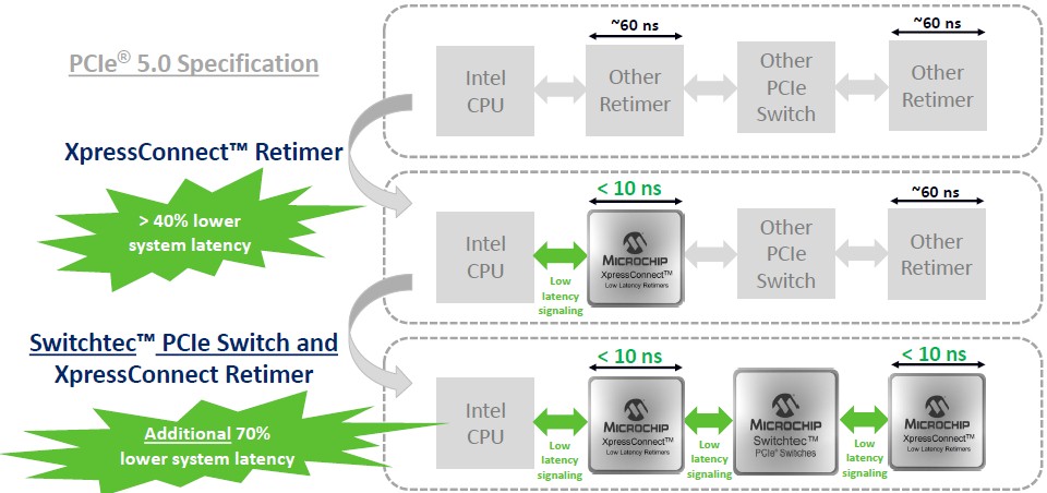
The PCI-Express 5.0 specification, which was largely controlled by Intel we suspect, says that the retimer latency has to be lower than 61.5 nanoseconds. We suspect that this is the case because if it is any higher than that, the Compute Express Link (CXL) interconnect that Intel is pushing for asymmetrical shared memory connections between CPUs and peripherals like FPGAs and GPUs may not work well. Presumably there will be other retimers, and they will meet the spec and not exceed it, and Jang’s chart certainly implies this. Now, if you drop one of these other retimers in between the CPU and the PCI-Express switch and another between the PCI-Express switch and the next retimer, which presumably will hook to the in-chassis peripheral, that is around 120 nanoseconds of total retimer latency just for the retimers. The Microchip XpressConnect retimer runs at under 10 nanoseconds of latency, and that is probably on the order of an 85 percent reduction in latency in this simple scenario.
What this chart, and none of the spec sheets, from Microchip does not tell you is the latency of a port-to-port hop through the Switchtec switch ASIC itself, and as it turns out, it is on the order of 100 nanoseconds to 120 nanoseconds for the PCI-Express 4.0 version and we highly suspect that the latency will not be any lower with the PCI-Express 5.0 version. There just is not a lot of room to lower it, any more than there is with InfiniBand. That said, this latency is a lot higher than some of the figures that PCI-Express switch makers have been citing – we are not sure why, but would they count only half of the hop? – and is absolutely consistent with the latency of an InfiniBand switch ASIC. And, importantly, the Switchtec ASIC latency is much better than an Ethernet switch ASIC, which is anywhere from 350 nanoseconds to 450 nanoseconds for a fast one and even higher for a slow one. So the end-to-end latency for the Microchip solution is on the order of 120 nanoseconds to 140 nanoseconds. A “Skylake” Xeon SP server accesses the local DDR4 DRAM on its socket in about 89 nanoseconds and in a two-socket system in about 139 nanoseconds across the UltraPath Interconnect link between the CPUs; L3 memory access is on the order of 20 nanoseconds. (We talked about this back in 2017.) The point is, if you have slower PCI-Express retimers and a slower PCI-Express switch, then it will be potentially 2X to 3X slower than main memory access – defeating the purpose of CXL, if you think about it.
We will be very interested to see what Broadcom cooks up in response to this Switchtec PCI-Express 5 plus XpressConnect combo, and how the Microchip and Broadcom offerings are picked up by server, storage, and composable fabric makers.
To help you get a handle on the three generations of Microchip Switchtec PCI-Express switches, we built this handy little table and calculated the bandwidth based on the lane count and some initial specs with the top-bin PCI-Express 3.0 switch from several years ago. It is not clear why aggregate bandwidth – the most basic thing in a switch – is not shown for each SKU in the spec sheets. It is also not clear why the PFX 96xG3 ASIC is rated at 174 GB/sec when by our math it should have a peak 192 GB/sec bandwidth across 96 lanes. We assume, then, that the 174 GB/sec is actual bandwidth achieved relative to peak. We just doubled up the lane speeds and counted up the lanes per SKU to fill in the rest of the table. Take a gander:
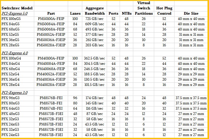
A couple of things jump out here. First, each generation has two physical chips: a big one and a slightly smaller and less capacious one, and then there is the usual bin sorting to use partially dudded parts. We have no idea what watts these things burn or what manufacturing processes they use or how many transistors they have. Second, there is a lot of bandwidth in these boxes. And third, we think in some cases companies will want to increase the radix of the chip by splitting the ports in half with the PCI-Express 5.0 generation, doubling up the effective port counts to hang more devices off each switch. Not everyone, mind you. But many.
There are a couple of other things you need to know about Microchips’ Switchtec line. First, with the PCI-Express 4.0 version, it had a special SKU called the PAX that actually included a software fabric, akin to what GigaIO and Liqid sell, that was embedded in the switch. Think of it as a fabric accelerator with microcode on it. While Jang is making no promises, we highly suspect there will be a PAX variant for the PCI-Express 5.0 version.
The other neat thing is that the Switchtec line supports a bunch of different topologies. There is a cross domain link that lashes two switches with each other very tightly that has limited scale but a lot of bandwidth between those two devices. The PCI-Express switches support ring, mesh, and fat tree topologies, but Microchip has not done a torus or dragonfly interconnect as yet. But it could if customers want it.
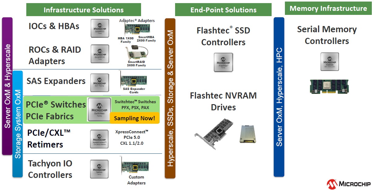
You may or may not be familiar with Microchip, so here is a summary table of its product families, which come from various acquisitions:
IBM tapped Microchip to make the DDR4 memory buffers that were used in its experimental (and never launched) Power9’ kicker processor to the Power9 systems, the former which was due in 2019 and the latter which launched in late 2017. IBM is also tapping Microchip to make the memory buffers for its DDR5 memory, which has a lot of interesting bandwidth and latency tweaks that make it competitive with HBM2 memory without a lot of the grief. That memory controller and buffer chip is shown in the chart above along with the DDR5 memory that IBM expects to use in conjunction with its SERDES-based OpenCAPI Memory Interface (OMI) on the Power10 chip to create a “memory area network.”


This sentence: “We suspect that this is the case because if it is any higher than that, the Compute Express Link (CXL) interconnect that Intel is pushing for asymmetrical shared memory connections between CPUs and peripherals like FPGAs and GPUs.” is leaving me a bit confused. Can you clarify?
Hi Steven
Thanks for the comment. The idea I was trying to get out is that you need low latency interconnects for things like CXL to make remote memory look close like DRAM is in the CPU. Nvidia had to create NVLink to get this same effect with Power9 processors from IBM, for instance. (I realize CXL and NVLink are very different animals.) If the retimers take 60 nanoseconds and you need two of them to get distance between the CPU and the peripheral and the switch is taking on the order of 100 nanoseconds to 120 nanoseconds, then you are up to 220 nanoseconds to 240 nanoseconds for access from CPU across CXL to the device compared to, what?, maybe 90 nanoseconds for local CPU memory and 140 nanoseconds for remote CPU memory in a two-socket NUMA box (using monolithic Xeon SP processors). Average it out, and that CXL-attached memory in a GPU or FPGA or whatever is 2.5X times further away than the CPU memory inside the box with retimers that just adhere to the PCi-Exprtess 5.0 spec minimums. That may be a latency bridge too far for things to look seamless. With Microchip’s retimers plus its switch chip, you are on the order of 120 nanoseconds to 140 nanoseconds for that CXL memory access — almost the same as the CPU itself. Much smaller gap.
@Timothy,
First sentence tense error.
“If the datacenter has been taken over…”
“has” –> “had”.
Correct! Thanks.
Not one mention of amd even though they are the only cpu with pci express 4.0 currently out in the wild lol….not counting power just x86
Well… I was talking about a switch, not a server. And PCI-Express 5.0, not PCI-Express 4.0. Everyone will have PCI-Express 5.0 soon and then we can have some fun.