

It must have been something in the cosmic ether.
Apopros of nothing except the need to fill a blank page with something interesting back when we were analyzing IBM’s second quarter financials and considering the options that Big Blue has with the “Cirrus” Power10 systems it will be launching about a year from now, we did a thought experiment about what it would mean if IBM started to believe in big iron machines again. And to be really precise, we suggested that IBM take some of the ideas borne out in the Parallel Sysplex memory clustering for its System z mainframes and adapted it to create giant shared memory clusters based on Power10 nodes.
And as it turns out, this is precisely what IBM is doing – with some interesting twists.
Bill Starke, the chief architect of the Power10 chip, had something between a good laugh and a mild cardiac arrest – had we hacked into his laptop? – in reading our suggestions about bringing something like Parallel Sysplex to Power10 back in June, especially when we suggested that IBM could span 6,144 cores and up to 2 PB of memory in a giant, wonking, shared memory NUMA system using current Power9 chips. As it turns out, the Power10 actually has 51-bit physical addressing and a cluster of its processors can indeed see an address space that is 2 PB in size – if enough nodes with enough DDR memory slots are lashed together in the right way.
As far as we know, no other CPU out there can do that. The current “Cascade Lake” and “Cooper Lake” Xeon SP processors have 46-bit physical addressing (64 TB) and 48-bit virtual addressing (256 TB) – and the value of the latter is questionable. Intel’s Xeon SPs have more than just one memory bottleneck, but three: too few memory controllers, which limits both memory capacity and memory bandwidth at the socket level, and memory addressability, which limits the capacity (and therefore the bandwidth) across multiple sockets in a shared memory system using either symmetric multiprocessing (SMP) or non-uniform memory access (NUMA) clustering.
We hinted at the memory clustering technology that is at the heart of the Power10 architecture – what IBM calls “memory inception” and what we are calling a “memory area network” in our initial coverage several weeks ago in our review of the Power10 presentation at the Hot Chips 32 event. We promised to circle back and get into the details of the Power10 memory architecture and its massively scalable shared memory features, and talk about the ramifications it could have on enterprise, cloud, hyperscaler, HPC, and AI computing individually and as a group. This could be a game changer for IBM, if not amongst the hyperscalers then for its own IBM Cloud if it really believes in its own technology as it should.
Thanks For The Memory
We will take this step by step, because this is fun if you like system architecture. (And we do here at The Next Platform.)
As we have pointed out before when talking about the still-not-seen experimental Power9’ “Axone” processor, back in October 2019, and the hints about the design of the Power10 processor we got from an in-depth interview with Starke, back in August 2019, the shift from dedicated DDR4 memory controllers to Serdes-based, high speed differential signaling mixed with buffer chips on memory modules that can be taught to speak DDR4, DDR5, GDDR6, 3D XPoint, or whatever, is an important shift in system design and one that we think, ultimately, the entire industry will get behind eventually. The flexibility and composability benefits that Big Blue will be demonstrating with Power10 systems are just too big to be denied or ignored.
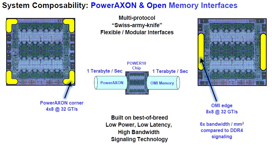
Let’s take a look at the OpenCAPI Memory Interface, or OMI, and the PowerAXON I/O interfaces, formerly known by the code-name “BlueLink” on the Power8 and Power9 processors. Examine below:
From the old roadmaps that we saw in recent years, it looked like IBM was planning to support 32 Gb/sec and 50 Gb/sec speeds on the next-generation BlueLink ports on the Power10 chips, up from 25 Gb/sec on Power8 and Power9. Our guess is that this would be done mostly through the addition of PAM-4 pulse amplitude modulation encoding on 16 GHz and 25 GHz SerDes. PAM-4 encoding is being done on switch ASICs to double up the bandwidth per clock on those ASICs. (Non-zero return, or NRZ, encoding used for various network transports can put one bit inside a signal, but PAM-4 can do two bit per signal.)
From the chart above, it sure looks like IBM just went with 32 Gb/sec signaling across the board, probably just using 16 GHz native signaling it already had in the Power8, Power9, and Power9’ chips for the NUMA interconnects and adding PAM-4 encoding to it. The expected upgrade to BlueLink running at 50 GHz and delivering 50 Gb/sec (25 GHz plus PAM-4 encoding) did not happen, apparently, and we think after IBM went back to the drawing board and very likely after it was clear that Nvidia and IBM were not going to win the two big exascale supercomputer deals in the United States, it just dropped all of the signaling back to 16 GHz with PAM-4. NVLink 3.0, as we have talked about recently in our overview of the “Ampere” A100 GPU architecture, runs at 25 GHz with PAM-4 encoding to yield 50 GB/sec of bandwidth across four ports.
As we said a few weeks ago, we think IBM was planning on supporting those two BlueLink speeds (32 GT/sec and 50 GT/sec) on a chip with 24 skinny SMT4 cores or 12 fat SMT8 cores, and very much like the Power9’ machine, and Power10 was essentially a new core that would be plunked in this design and then it would create dual-chip modules (DCMs) to boost the core count to 48 per socket. At some point, when IBM decided to really push the core design and put 32 skinny SMT4 or 16 fat SMT8 cores on a die, it looks like IBM also decided to do away with the faster 50 Gb/sec speeds used for some of the BlueLink ports (used for NUMA links between sockets or within sockets and as well as OpenCAPI ports) and just make all of its differential signaling SerDes run at 32 Gb/sec.
Making all of the I/O Serdes the same, or as much as possible, makes sense, and gives IBM great flexibility in terms of what it can connect to the Power10 processor complex, and the protocols it can use to do it. IBM calls these different blocks of signaling by different names – OMI and PowerAXON – but we think the only difference is the protocols that are enabled on top of them.
What IBM did do, at least for the 16-core Power10 implementation of Power10 that was shown at Hot Chips 32, was take eight BlueLink SerDes with eight lanes a pop and turn that into two OMI memory controllers, which you see on the left and right of the Power10 die on the chip above with an aggregate of 1 TB/sec of aggregate bandwidth. The PowerAXON interfaces are on the corners, and they have four SerDes with eight lanes each, which at the same 32 GT/sec per lane add up to 1 TB/sec of aggregate bandwidth. The BlueLink signaling running at 32 Gb/sec has six times the bandwidth per square millimeter of area as DDR4 memory controllers that IBM created for the Power9 processors and would have otherwise shrunk from 14 nanometers to 7 nanometers in the Power10 generation. The Power9’ test chip was etched in 14 nanometers, and this is where this comparison really comes from, as we showed here. It is still possible that IBM will roll the Power9’ out in Power Systems Advanced I/O machines – or Power AIO for short – between now and the end of summer or beginning of fall next year when the Power10 ships. The availability of buffered DDR4 or DDR5 memory, which requires the buffer to be made by MicroChip and for a DIMM maker to make the memory sticks using it, is probably the factor that is holding this Power AIO machine from being launched. (That’s just a guess.)
These differential signaling SerDes are extremely useful, and we think, in the fullness of time, this is how all I/O will be done on processors because of what Big Blue has done with Power9’ and will be doing with Power10. We discussed this two years ago, when we wrote after the Hot Chips 30 presentation, that IBM was blurring the lines between memory and accelerators with its BlueLink architecture and went into a lot of details about these SerDes.
The main point to remember when considering this – and we have read the riot act to every CPU maker that we know – is that there is no reason to hard code the memory and I/O on a chip ahead of time. This should be done on the fly, with generic signaling, allowing customers – or at least server vendors – to determine the ratio of memory and various kinds of I/O that attach to their processing complexes. There is no longer a good reason for these to be fixed. If I want a CPU that is mostly a memory monster, then I will make most of the SerDes speak to the memory buffers, which in turn will translate that into DDR4, DDR5, or DDR6 as needed. If I want a CPU that has lots of different peripherals, then I will configure that signaling to speak plain OpenCAPI BlueLink or NVLink or whatever.
At the moment, IBM has not converged down PCI-Express 5.0 with the Power10 chip to its BlueLink SerDes, and it is not clear why. Power10 has two discrete PCI-Express 5.0 controllers for a total of 32 lanes, and IBM says in its presentation that in a Power10 DCM, the socket has 64 lanes (four controllers) running at 32 GT/sec. In the past, the difference between BlueLink ports and NUMA ports and PCI-Express ports used to be speed. With the Power9 chip, for instance, PCI-Express 4.0 controllers ran at 16 GHz and the local NUMA links spanning up to four sockets also ran at 16 GHz while the BlueLink ports (including those supporting Nvidia’s NVLink protocol and those supporting remote NUMA links to scale out to 16 sockets in Power Systems) ran at a faster 25 GHz. The local NUMA links had 32 lanes and the remote NUMA links had 24 lanes. Our point is this: PCI-Express 5.0 runs at 32 Gb/sec, just like the updated PowerAXON and OMI BlueLink ports, so go figure. There are probably things that the PCI-Express controller needs that BlueLink doesn’t have, or the native PCI-Express 5.0 controller design was more energy efficient or more energy efficient or just plain done and easy.
Here is an important image to consider when thinking about Power10:
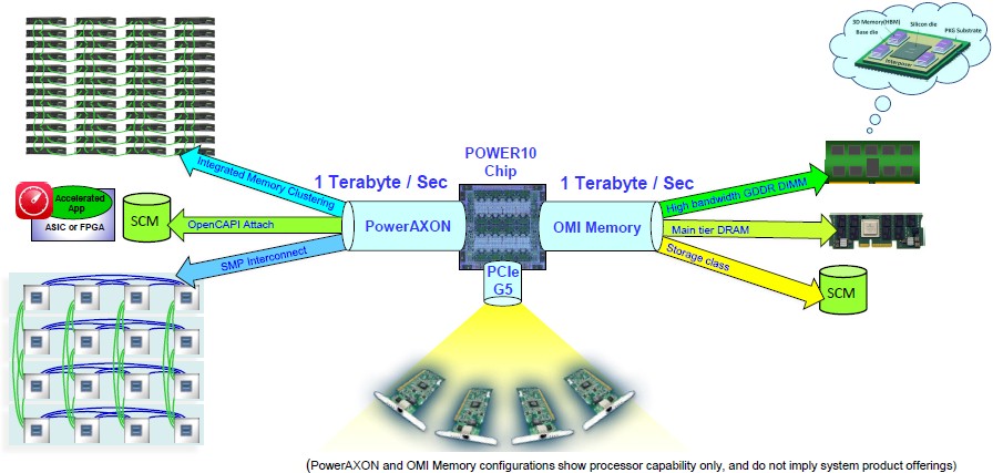
There are a lot of things to consider in this chart, so let’s step through it. Coming out of the right side is the main tier DDR4 DRAM memory, which can scale up to 4 TB per socket across those pair of OMI SerDes left and right on the Power10 chip, and can deliver 410 GB/sec of bandwidth (presumably at DDR4-3200 speeds of 3.2 GHz) using the DDR4 buffer chip from MicroChip and only adding a mere 10 nanoseconds to memory latency. And when DDR5 memory is out, customers will be able to still use the OMI SerDes to drive it, and MicroChip will come out with a new buffer that translates the differential signaling to the DDR5 protocol.
These OMI interfaces will also, in theory, allow for the attachment of storage class memories – think 3D XPoint or PCM that are byte addressable like DRAM – and this is where that 2 PB addressable space will come in handy in many scenarios. When and if Micron Technology and others get persistent memory out the door. Right now, Intel has a lock on 3D XPoint (really a tweak of ReRAM) memory in DIMM form factors, but that won’t hold forever. The other interesting scenario you see on the right hand side of that chart above is a hypothetical GDDR6 memory module, which could supply up to 800 GB/sec of sustained memory bandwidth, nearly filling that 1 TB/sec of aggregate bandwidth in the OMI SerDes pipes and delivering a little more than half of the 1.55 TB/sec bandwidth of the HBM2 stacked memory that an Ampere A100 GPU accelerator does – without the grief of memory stacking and an interposer and packaging substrates to link that HBM2 memory to the CPU complex.
This is a very interesting possibility, indeed.
On the left hand side of the chart, we see the faster NUMA interconnects implemented with the PowerAXON ports – IBM calls them SMP links, but they are not SMP because all memory accesses are definitely not the same distance away in space and therefore time in the compute cluster and the memory is not all bunched together and accessed over a bus or crossbar, either, as SMP designed used to do. Memory is not only local to a socket, but has locality of a sort to each section of the OMI SerDes on the die. Even if every Power10 core in a complex with 240 fat cores (and possibly 480 skinny cores) can access any main memory in a system with as many as 256 OMI SerDes banks and up to 2 PB of memory, and even if the local and remote NUMA links now run at the same speed (32 GHz), the distances are not the same and therefore the latencies will not be precisely the same as a machines expands its CPU and/or socket count. But this is a much more balanced design than Power8 or Power9, to be sure.
These PowerAXON links also support the attachment of storage class memories in “device form factors,” as IBM put it, using the OpenCAPI interface. (And interestingly, IBM is not supporting Intel’s CXL protocol over PCI-Express 5.0 controllers because it says OpenCAPI is superior in that it provides true coherence and data encryption to boot.) Those OpenCAPI links can also be used to attach FPGAs to the Power10 complex as well as other ASICs – provided they support OpenCAPI. And if not, IBM and partners can lay down a baby FPGA onto the device card that implements the OpenCAPI interface in programmable logic and make it look native-ish.
And that leads us to the “memory inception” capabilities on the upper left of this chart. With memory inception, IBM says it “enables a system to map another system’s memory as its own” and that “multiple systems can be clustered, sharing each other’s memory.”
Like we said, a memory area network.
This capability, according to Starke, has its origins in the global memory addressing in the PERCS project with the US Defense Advanced Research Projects Agency, which funded IBM’s Power7 development for the Power 775 supercomputer nodes used at many national HPC labs as well as the never-installed IBM implementation of “Blue Waters,” which had a very dense pack of these machines but which IBM canceled because the machine was too expensive to build. The University of Illinois went with a hybrid CPU-GPU machine from Cray, and got the $188 million. There is a certain amount of insight that was brought in from the System z team and the Parallel Sysplex design as well to create the Power10 memory area network.
“This is better than any memory cluster,” Starke tells The Next Platform. “This is true memory disaggregation, where you can literally borrow the memory for another server on the other side of the cluster and all of the protocols just flow over to there as if that memory was directly in your system. There is a minor latency due to NUMA aspects, on the order of 50 nanoseconds to 100 nanoseconds, which is within reason for something that doesn’t require customers to rewrite one bit of their software.”
We begin to see why Google was interested in joining the OpenPower Consortium way back when. Perhaps Google might have stuck around for this bit. Perhaps all CPU makers are working on this. We shall see. We think now they have to.
Here is one simple example of how memory area networks might be used in Power10 pods:

This is an example that just shows borrowing of memory across nodes, where different workloads are configured with memory across different servers such that some of the nodes become, in effect, memory servers for the other nodes – and in a dynamic fashion, presumably.
But you can take this in very different directions. Here are two different memory area network topologies that push it to two different extremes:
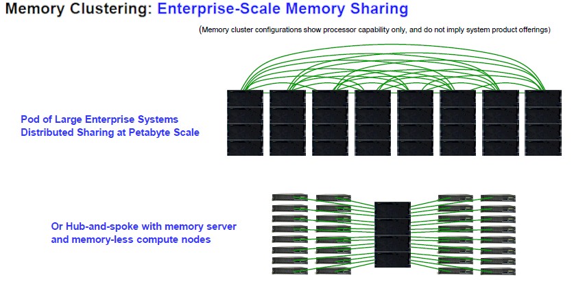
In the top setup, eight large Power10 big iron boxes are lashed together with their PowerAXON cables that allows them to have a distributed, shared storage pool that is on the scale of petabytes. It is not clear if the operating system can see all of the compute and all of the memory as a single NUMA machine, but that is the implication and that is astounding if you think about it. And it is at exactly the 32 server limit of Parallel Sysplex to get to 2 PB at 4 TB per socket at 16 sockets per big box, by the way. (See, told ya.) So that picture shows only a quarter of what IBM can do.
The bottom part of the chart above interesting, but for a different reason. In this case, a big fat Power10 NUMA box with 64 TB of memory is essentially a memory server for 32 entry Power10 server that have no physical memory of their own, but can access anywhere up to 64 TB individually as workloads require it. This is the kind of thing that the Gen-Z people over at Hewlett Packard Enterprise have been saying is the future, and IBM is doing it with a memory interconnect right off the CPU.
Now, here is where it gets really cool, and why we call it a memory area network. (You’re welcome, IBM.)
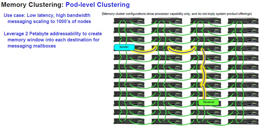
“You can take it to the next stage once you can share memories between neighbors, and you can go multi-hop,” says Starke. “I can build an integrated cluster just by reading from memory in one node and writing to memory in another node. And the hardware will automatically route that across the entire datacenter, scaling up to thousands of nodes, and you are basically building the moral equivalent of an InfiniBand network here with extremely low latency and extremely high bandwidth and the scale of that is really only limited by that upper memory limit of 2 petabytes.”
Now, IBM didn’t think of it this way, but imagine if you took half of the Power10 CPUs out and had NVLink coherence between a Power10 CPU and a kicker to the Ampere A100 GPU, or even the Ampere GPU itself. The memory area network on the Power10 CPUs could provide a huge memory space for both the CPUs and the GPUs to play with, thanks to the coherence IBM already has across NVLink (which is really BlueLink running a slightly different protocol that makes the GPUs think DRAM is really slow but really fat HBM2, in effect, and also makes the CPUs think the HBM2 on the GPUs is really skinny but really fast DRAM). And IBM could have introduced a more capacious and less costly memory tier as well, with the use of GDDR6 memory cards. Or, if cost was an issue, Nvidia and IBM might have been able to make a much simpler and less costly exascale machine using shared GDDR6 memory using OMI interfaces on both the CPUs and the GPUs with big banks of DRAM for capacity, and the resulting machine could have been so much more malleable than either the “Summit” machine at Oak Ridge National Laboratories or the “Sierra” machine at Lawrence Livermore National Laboratory – and potentially not required Nvidia’s NVSwitch at all. All that would have been required is for IBM to add some 50 Gb/sec BlueLinks running the NVLink protocol to link into Ampere, or for Nvidia to offer a version of Ampere that could downshift to 32 Gb/sec if that is all IBM could do with OMI and PowerAXON links.
To one way of thinking, making a more malleable and flexible machine was more important than packing the most flops possible in a box for the lowest price. But the political status and technical pinnacle come from getting those flops on the cheap. All we are saying that there is a chance that this architecture might turn out to be better. And maybe it will take IBM on its cloud or Google on its cloud to prove it. If Big Blue really believes in its technology, then it should build an exascale-class supercomputer from Power10 and a bunch of Nvidia GPUs and prove that it is right, and then sell it by the slice like New York City pizza.
Nvidia was in the middle of buying Mellanox Technology when these two exascale deals were being finalized, and it probably would not have made Mellanox (and therefore Nvidia) happy to see an exascale machine built without InfiniBand. But clearly it could be done, and for all we know, this is what IBM proposed. We have nothing against awarding the Department of Energy deals to Cray (now part of Hewlett Packard Enterprise) and using future AMD Epyc CPUs and Radeon Instinct GPUs plus cray’s Slingshot interconnect to lash nodes together. But just think that there is another way to skin this exascale cat, and it is the job of the national labs to adopt different approaches and in this case, if there is a fourth exascale machine that is funded, it should be something based on Power10 and a memory area network with GPUs sharing memory with CPUs (both DRAM and maybe HBM2 and GDDR6) across that memory area network. Considering what we are investing already, and the learnings that could come from this, why not?
But again, it would probably be best if IBM and Google built it, much as Google has built TPU pods for running AI workloads. Google and IBM have enough money to do this themselves, and give the national labs a run for both the HPC and AI money. All the work has been done in the hardware. Now it is down to systems software and applications, as always.

Another Crazy Idea: Intel Might Buy Globalfoundries
Back in March, when we wrote up Intel’s Integrated Device Manufacturing 2.0 strategy put forth in the vaguest of terms by then-new chief executive officer Pat Gelsinger, we quipped that Intel might be wishing as it launches Intel Foundry Services that it had some of its older fabs around with …
IBM Bets Big On Native Inference With Big Iron
Everyone knows that machine learning inference is going to be a big deal for commercial applications in the years ahead, but no one is precisely sure how much inference is going to be needed. There is, however, an increasing consensus that for enterprise customers – as distinct from hyperscalers, cloud …
Red Hat Woos VMware Shops With OpenShift Virtualization Engine
Broadcom’s $61 billion acquisition of VMware in November 2023 and the subsequent changes to venerable virtualization company’s business model and pricing have rankled many long-time enterprise users, a situation that has been highly publicized despite assertions by Broadcom and VMware executives that such reports are little than FUD – short …
“3D XPoint (really a tweak of ReRAM)”.
While your architectural speculations are highly enjoyable and can be be spot-on (as the one on Power10 was) – you ought to get real data on what should not have to be speculation.
3-D Xpoint is Phase Change Memory. Its same fundamental memory for both Intel and Micron in terms of silicon (in fact Intel is currently buying it all from Micron, who owns the Fab). No one else has any persistent memory in production.
ReRAM has always been and will likely always be an “emerging” memory. The papers from Micron prove how and why its impossible to make any product out of ReRAM. HP is the most prominent failure after backing it, after relentlessly hyping ReRAM as a “memristor”.
I thought the consensus was that it was a variant of ReRAM and was not a spin on PCM… See: https://www.theregister.com/2015/07/28/intel_micron_3d_xpoint/
And:
https://en.wikipedia.org/wiki/3D_XPoint
Not that I necessarily trust Wikipedia, mind you. I have not seen the papers you refer to.
And of course, there is this statement:
https://thememoryguy.com/emerging-memories-today-the-technologies-mram-reram-pcm-xpoint-fram-etc/
Yes, there is no authoritative documentation outside of the branding, so I’ll point you to these pieces instead.
https://archive.eetasia.com/www.eetasia.com/ART_8800718995_499486_NT_dcd3d606.HTM
The papers I referenced are available in IEEE Explore, presented at IEDM and such premier conferences from some 2-4 years ago. Its too bad the researchers and companies hype up the “memristors” and such, to mislead people in order to sell their papers. We probably have more ReRAM papers than actual ReRAM bits ever produced.
Very impressive, having an ability for the cores of one node being able to access scads of terabytes of memory residing both locally and remote. But this article left me with a question. Are accesses fully cache coherent across the memory cluster or does cache itself need to be managed by software?
For example, picture a workload running only on the cores of a Node A. I would expect that, no matter the source location of the memory, the cores in Node A would be capable of moving data between their own caches in a cache coherent fashion (i.e. no involvement by software). But now picture some IO device on Node B altering some part of the memory being used by the workload running on Node A, say simply reading a page from persistent storage or packets from some communications device. Did the caches of the cores on Node A see the change such that their associated cache lines were invalidated? Would subsequent accesses of the remote memory-mapped real address space by Node A then access the changed data in Node B?
Or suppose we go in the other direction. Suppose that some of the pages of that memory remote from Node A but residing on a Node B need to be written to some IO device, say an SSD array. The IO device on Node B drives the write to the SSD. But let’s have a cache on Node A holding changed data normally residing in the memory of Node B and it is that changed data that needs to be included in the IO write. Did the cache on Node A automatically see the need for its data to be included in the IO write or is there first a need for software to force the cached/changed data back into Node B.
Again, impressive, but there are software architecture aspects of this that might need to be factored in to be able to use such massive memory in a single workload, even if it is running just on one node. Can anybody comment on the level of cache coherence actually supported here?
As you might imagine, we would love for you to take a hard look at this and give us your thoughts, Mr Funky. Hope you are well.
Probably Mark’s last name is better written without a final trailing y.
I would imagine that memory gets partitioned somehow between processors so that cache invalidation messages don’t overwhelm the memory interconnects at scale. How flexible this is would be an interesting topic to report on. Given how innovative the hardware is, I find it strange that IBM still seems to focus their marketing efforts on nontechnical business types rather than the engineers that the sensible decision maker relies on for guidance.
Along slightly different lines, as demonstrated by the ascent of x86 and now ARM, it seems the way up involves getting a bunch of young developers involved in writing software. As a significant amount of software these days is written on single-user desktops and notebook computers, it seems unlikely that Power10 will become popular at large scale unless it first becomes affordable at small scales.
Unfortunately, having a separate memory controller attached through a fast SerDes link may increase prices on the desktop beyond Power9, which was already too expensive to be attractive to software developers.
My vote for an affordable, entry-level system is based on a heartfelt desire for the modern power architecture to become popular enough that it survives into the future.
First, doing fine. Got asked back to teach DB, architecture, and a class on the first part of any development process, all remote. Students seem to like it. Great retirement “job”. As to this machine’s programming storage model, I’d love to. I need a connection or two though. I know Mr. Starke and he might still know me from IBM i, but could I ask you to make (re)introductions to folks there in the know? I can take it from there.
This wiki description indicates an “up to” 52 bit physical address space capability for Ice Lake. Did Intel go into details of this for the Ice Lake Server implementation, recently presented at Hotchips 2020?
“The 5-level paging scheme supports a Linear Address space up to 57 bits and a physical address space up to 52 bits, increasing the virtual memory space to 128 petabytes, up from 256 terabytes, and the addressable physical memory to 4 petabytes, up from 64 terabytes.[14][13]”
https://en.wikipedia.org/wiki/Ice_Lake_(microprocessor)
Fascinating read on the Memory Area Network of IBM’s Power10! It’s great to see the details on how this innovative architecture is capable of delivering such high performance and efficiency. Definitely looking forward to seeing the real-world applications of this technology in the future.