

The system world would have been a simpler place if InfiniBand had fulfilled its original promise as a universal fabric interconnect for linking all manner of devices together within a system and across systems. But that didn’t happen, and we have been left with a bifurcated set of interconnects ever since.
Let’s rattle them off for fun.
There are the memory buses that link DDR4 and HBM2 memory to processors. There is some agreement on how to etch controllers for these memories, since they all have to speak the same physical memory, but there are still many different memory controller designs.
There are NUMA interconnects between sockets in a single physical machine as well as NUMA interconnects that span multiple server nodes to create shared memory systems that span two, four, eight, or sixteen sockets. These are all largely proprietary, and have been for as long as there has been NUMA iron. (Nearly three decades.)
Then there is the PCI-Express bus and its accelerated forms. This includes NVM-Express acceleration for flash, which gets the CPU hosts out of the loop when the network wants to access data on flash as well as GPUDirect over PCI-Express, which link GPU memories to each other without host involvement in a similar fashion. AMD’s Infinity Fabric is a kind of superset of PCI-Express, borrowing techniques from its HyperTransport NUMA interconnect, to create a universal fabric for linking CPUs to each other, GPUs to each other, and CPUs to GPUs. Nvidia’s NVSwitch is a fabric that speaks load/store memory semantics that links GPU memories to each other in something akin to a NUMA setup, but just for the GPUs. (NVSwitch could, in theory, be used to create a switched fabric that links CPU memories to GPU memories provided that a CPU had NVLink ports on it, but thus far only IBM’s Power9 chips had such ports and NVSwitch was not used in this fashion.)
The CCIX accelerator interconnect uses the PCI-Express transport and protocol as its foundation, was created initially by Xilinx and then endorsed by AMD and actually adopted by Arm Holdings as an accelerator interconnect as well as a NUMA interconnect between Arm CPUs. It has been shown off in various Neoverse CPU designs, but has yet to be implemented in an actual volume Arm server chip.
IBM’s CAPI interconnect ran atop PCI-Express 3.0 or PCI-Express 4.0 transports, but the OpenCAPI interface runs on specialized high speed SerDes on Power9 and Power10 chips, circuits that are being used not only to link accelerators in a coherent fashion to Power CPUs, but also to link the DDR5 main memory in the impending Power10 chip to the processor.
The Gen-Z protocol out of Hewlett Packard Enterprise had its own way of linking a fabric of server nodes to a giant shared memory that we still think is interesting.
And finally, InfiniBand and Ethernet keep getting higher and higher bandwidth and have sufficient latency to do interesting things. But their latencies are still too large for creating coherent memory spaces for diverse compute engines to play in together.
Still, like time, bandwidth increases, latency drops, and the plethora of new protocols heal all wounds. And now, that diversity of interconnects is opening up the options for system architecture.
The resulting architectures might be more complex, but they are also potentially richer and also could result in the ability to not only co-design hardware and software more tightly in future hybrid systems and distributed computing clusters built from them, but to dial up the right combination of price and performance to meet particular budget requirements.
That is the impression we took away from a keynote address that Debendra Das Sharma, Intel Fellow and director of I/O technology and standards at Intel, gave at the recent Hot Interconnects 28 conference. Das Sharma gave an overview of the Compute Express Link, or CXL, interconnect that Intel has developed in response to the myriad accelerator and memory interconnects that have been put out there in the past decade. CXL came last, resembles many of the protocols mentioned above, and may not be perfect in all use cases. But it is the one interconnect that seems destined to be widely adopted, and that means we have to pay attention to how it is evolving. Das Sharma gave us an interesting glimpse of this future, which helps fulfill some of the ideas driving disaggregated and composable architectures — which we are a big fan of here at The Next Platform because it allows for the sharing of compute and memory resources and a precise (yet flexible) fitting of hardware to the application software.
It All Starts With The PCI-Express Bus
Although sufficient for its intended design as a peripheral interconnect for servers, the PCI-Express bus did not offer very high bandwidth for many years — certainly not high enough to link memories together — and importantly was stuck in the mud at the PCI-Express 3.0 speed for four or five years longer than the market could tolerate. Ethernet and InfiniBand were essentially stuck in the same mud at 40Gb/sec speeds at the same time until signaling technologies to push up bandwidth were painstakingly developed.
This is a great chart that gives you the transfer rates and latencies for the two broad types of interconnects, which you need to keep in mind as you think about any of these interconnects:
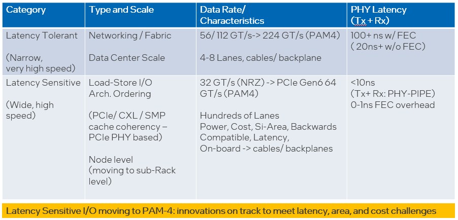
If you wanted to add another important dimension here, it would be the length of the possible connections between devices. But suffice it to say, low latency always implies short distance because of the limit of the speed of electrons in copper and photons in glass, and latency always increases with greater distance because of retimers, switch hops, and such.
The good news is that the next several generations at least between PCI-Express 4.0 and 7.0, it looks like we will see a two-year cadence of bandwidth increases with the PCI-Express interconnect, and PCI-Express switch fabrics that will have lots of bandwidth, reasonable radix, and with only a few tiers of switching will be able to span racks of gear pretty easily and, if bandwidth is held constant to drive up latency, could even span more than a few racks. This is all important in the context of the CXL coherent overlay for PCI-Express.
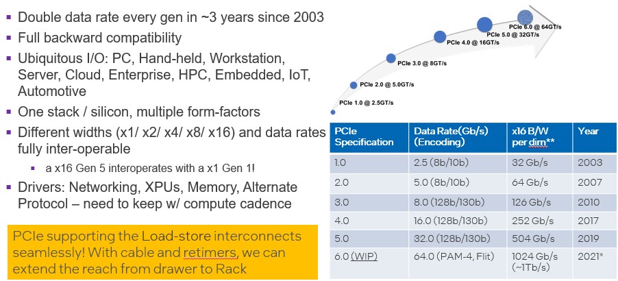
The PCI-Express 6.0 protocol, which we talked about in detail a year ago with Das Sharma, the bandwidth is going up through the addition of PAM-4 signaling, which has been implemented on several generations of datacenter switch ASICs already, and which encodes two bits in each signal coming out of the chip, thus doubling the effective bandwidth at a given clock speed. And the real clever thing is FLIT encoding and error correction, which is new and which has a lot less overhead than forward error correction does, and so the latency on PCI-Express 6.0 is going down, not up. And going down by half, which is just huge. And by shifting to a denser pulse amplitude modulation encoding — perhaps PAM-16 — the effective bandwidth can be doubled up again and latency dropped a bit with the PCI-Express 7.0 spec due around the end of 2023 and implemented probably two years later if history is any guide.
We did a deep dive into the CXL protocol two years ago, and we are not going to go through all of that again from the beginning. But this chart sums up the three elements of the protocol rather nicely for a quick review:
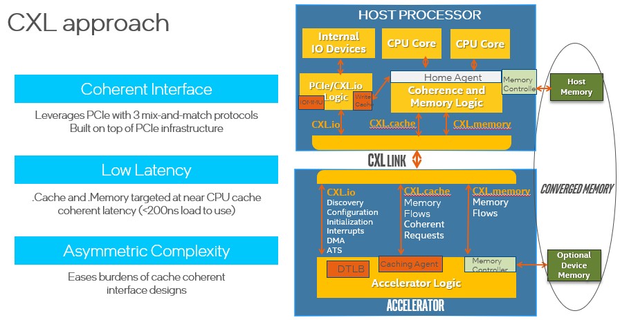
Here are the important things to consider. The CXL.io layer is essentially the same as the PCI-Express protocol, and the CXL.cache and CXL.memory layers are new and provide similar latency to that of SMP and NUMA interconnects used to glue the caches and main memories of multisocket servers together — “significantly under 200 nanoseconds” as Das Sharma put it — and about half the latency of the raw PCI-Express protocol itself. It is that latency drop — and further ones that we are expecting in the future — combined with the drumbeat cadence of bandwidth increases that makes CXL an interesting tool in the system architect’s toolbox.
The CXL protocol specification, in fact, says that a snoop response on a snoop command when a cache line is missed has to be under 50 nanoseconds pin to pin, and for memory reads, pin to pin as well, has to be under 80 nanoseconds. By contrast, a DDR4 memory access is around 80 nanoseconds, and a NUMA access to far memory in an adjacent socket is around 135 nanoseconds, according to system designers at Microsoft.
And as a further refresher, here are the three different usage models of CXL and the parts of the protocol they will use:

While the CXL 1.0 and 1.1 specs were about point-to-point links between CPUs and accelerator memory or between CPUs and memory extenders, as you can see from the use cases above, the forthcoming CXL 2.0 spec will allow a switched fabric that allows multiple Type 1 and Type 2 devices as shown above to be configured to a single host and have their caches be coherent, as well as allowing for memory pooling across multiple hosts using Type 3 memory buffer devices. This is what expands CXL from a protocol that links elements within a server chassis to one that links disaggregated compute and memory across a rack or possibly several racks — and frankly, puts CXL in some kind of contention with the Gen-Z protocol, despite all of the hatchet-burying that we have discussed in the past.
Economics will drive the pooling of main memory, and whether or not customers choose the CXL way or the Gen-Z way. Considering that memory can account for half of the cost of a server at a hyperscaler, anything that allows a machine to have a minimal amount of capacity on the node and then share the rest in the rack — with all of it being transparent to the operating system and all of it looking local — will be adopted. There is just no question about that. Memory area networks, in one fashion or another, are going to be common in datacenters before too long, and this will be driven by economics.
Das Sharma had some other possible future directions for the use of CXL in systems. Let’s go through them. The first scenario is for both memory capacity and memory bandwidth to be expanded through the use of CXL:

In this first scenario, chunks of DRAM are attached to the system over CXL and augment the bandwidth and capacity of DDR DRAM that hang off the traditional memory controllers. But over time, Das Sharma says that chunks of main memory could be put on the compute package itself — Foveros chip stacking is how Intel will do it — and eventually the on-chip DDR memory controllers could be dropped and just PCI-Express controllers running CXL could connect to external DRAM. (This is, in effect, what IBM is doing with its OpenCAPI Memory Interface, although it is using a proprietary 32Gb/sec SerDes to do it instead of a PCI-Express controller.) It is very likely that the on-package memory referenced in the chart above would be HBM, and probably not very much of it to reduce package costs.
The idea of memory that plugs in like a disk or flash drive is a long time coming.
In scenario two, CXL is used to create non-volatile DIMM memory for backing up all of main memory on in the system:
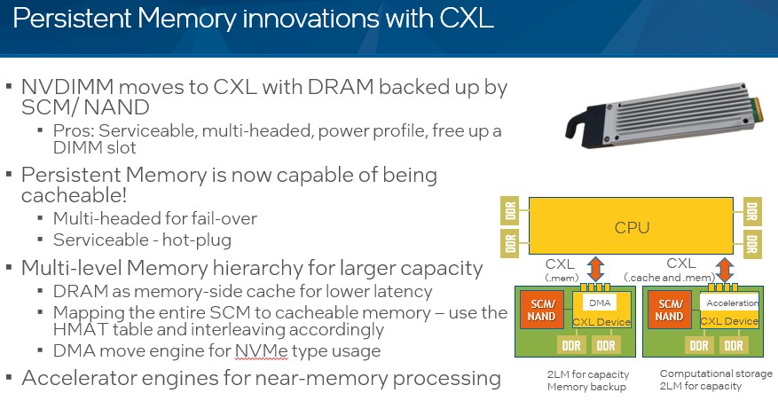
This NVDIMM memory is based on a mix of persistent memory (Optane 3D XPoint memory in Intel’s world) and DDR DRAM and, in some cases, this is converted to computational storage with the addition of local compute inside of the NVDIMM.
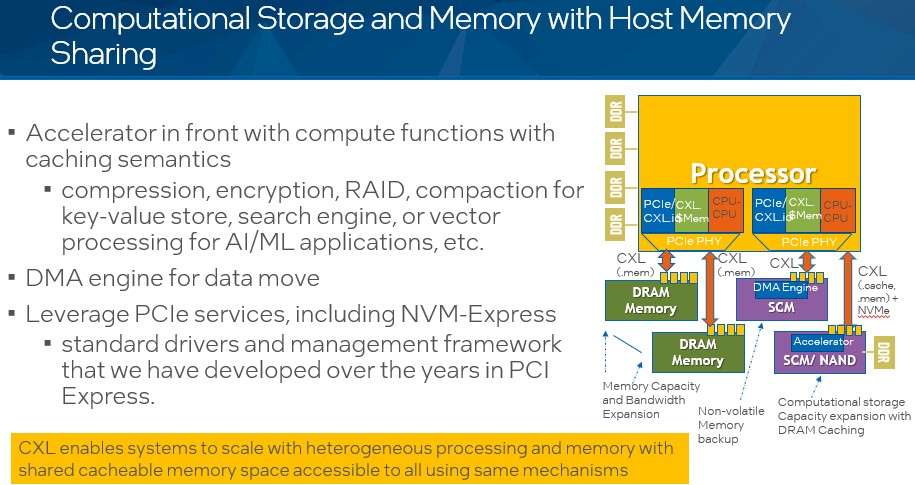
In scenario three that Das Sharma posited, the system will use a mix of CXL computational storage, CXL memory, and CXL NVDIMM memory, all sharing asymmetrically with the host processor’s DDR4 main memory using the CXL protocol. Like this:
And in scenario four, CXL disaggregation and composability is taken out to the rack level:
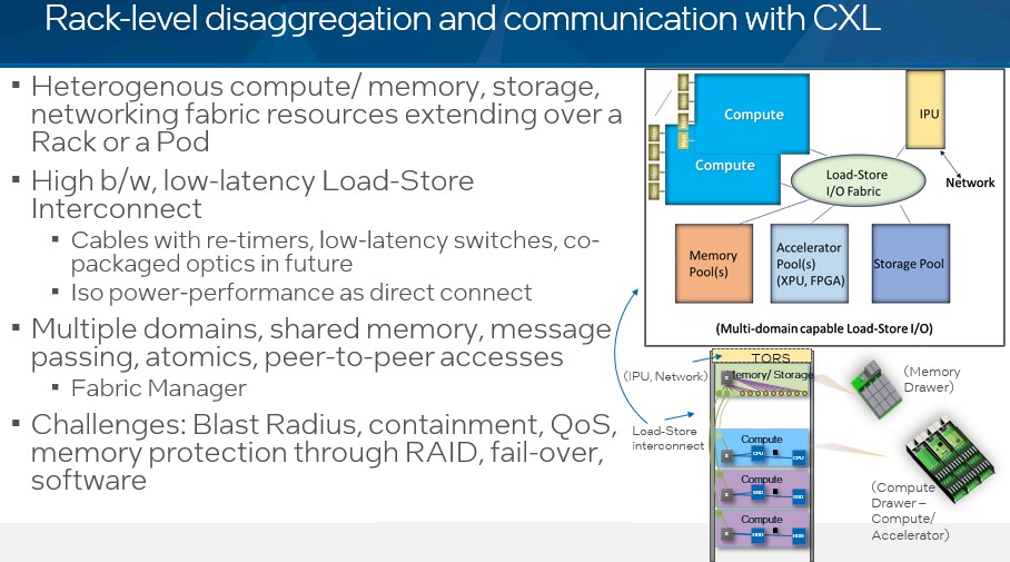
In essence, the rack becomes the server. There are some challenges that have to be dealt with, of course. But having a whole rack that is load/store addressable is very interesting indeed. It remains to be seen where the system software to control this will reside, but it looks like we need a memory hypervisor. Maybe Intel will snap up MemVerge and control this key piece of software as it develops.

With Gelsinger Gone, Who Benefits From An Intel Break Up?
We did not think that today we would be writing about Pat Gelsinger “retiring” from the company that he loves best and most. Intel’s prodigal and now former chief executive officer was one of the few executives in the semiconductor industry who was trained by the company’s co-founders Gordon Moore, …

Intel Shoots “Granite Rapids” Xeon 6 Into The Datacenter
UPDATED: Intel has been talking about its “Granite Rapids” Xeon 6 processors for so long that it would be easy to forget that they have not yet been formally announced. But today, the high end of the “Granite Rapids” server CPU lineup makes its debut, several weeks before AMD is …
The Datacenter GPU Gravy Train That No One Will Derail
We have five decades of very fine-grained analysis of CPU compute engines in the datacenter, and changes come at a steady but glacial pace when it comes to CPU serving. The rise of datacenter GPU compute engines has happened in a very short decade and a half, and yet there …
Interestingly, could CXL be a very good CPU-CPU board level interconnect too .. but it’s not mentioned in the Intel talk?
Shifting persistent memory (PM) to the far side of a CXL connector looks like a great idea, since PM tends to lag DRAM a bit in performance. You thus free up the CPUs’ scarce DDR slots for higher-performing DRAM, while allowing lots of PM in the same system.