

Based on what Intel has been saying for the past several weeks in various events, but especially the Hot Chips 2023 a few weeks ago and the more recent Intel Innovation 2023 extravaganza, the company’s foundry process roadmap and its server processor roadmaps are going to align harmoniously to make the Xeon SP family of CPUs more competitive next year.
We are not saying that Intel can close all of the gaps between itself and the Epyc alternatives from AMD or the various Arm alternatives from Ampere Computing and some of the hyperscalers and cloud builders who are designing their own server CPUs based on the Arm architecture. But it can move from being a supply winner – getting sales because it can ship a CPU, and just about any CPU using older manufacturing processes – to being a design winner – getting sales because its CPUs can compete on the technical and economic merits for specific workloads.
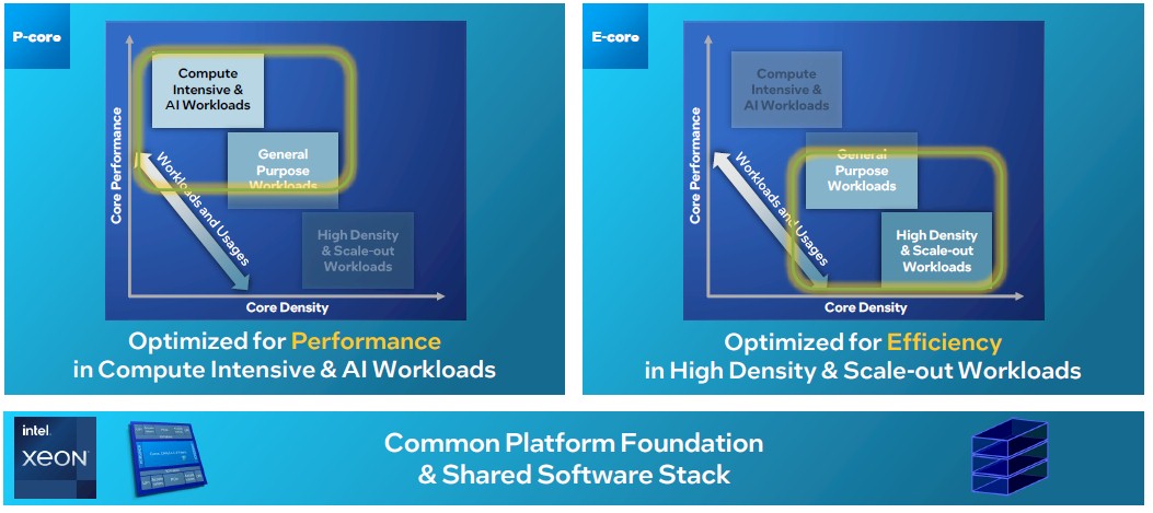
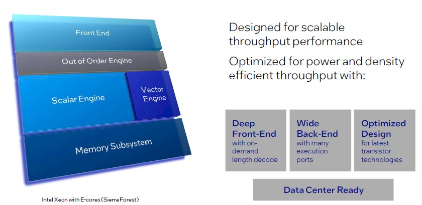
Intel has to cover a multi-front competitive landscape, and with its fat P-core and skinny E-core designs, which start rolling out next year, it will be able to do a much better job than it has been able to do in the past.
Of course, this is not the first time that Intel has fought a multi-front server war with different cores, nor is it the first time that AMD has, either. Both Intel and AMD have had fat and skinny cores in their architectures in the past, but this time is different. Intel’s Atom family for client devices was given wonking 512-bit AVX vector engines, ECC memory scrubbing, server-class virtualization, and other features and became the foundation of the “Knights” family of many-cored processors aimed at HPC workloads in 2015. And, for AMD, the “Seattle” Opteron A1100 processors, which launched in January 2016 as the dying gasp of the Opteron server chip line, was outfitted with low-power Arm Cortex-A57 cores at a time when its “K12” effort was going to create beefier, higher-end Arm server CPUs with the Opteron brand and in the designs that would also offer X86 cores with an EDA global replace. (That never happened.)
For Intel and AMD, this time is different because big server buyers – namely the hyperscalers and cloud builders – and the original equipment manufacturers – Dell, Hewlett Packard Enterprise, Lenovo, Inspur, Huawei Technologies, and Cisco Systems are the big ones – have all told Intel and AMD to innovate within a server platform, not across so many different server platforms. They want options within the socket, not across server architectures.
And so, it is no coincidence that this year AMD has versions of the fourth generation Epyc processors – generically part of the “Genoa” generation but with sub-codenames like “Bergamo” and “Siena” – with fat Zen 4 or skinny Zen 4c cores (the big difference being the amount of L3 cache attached to the core) and Intel will have versions of its fifth generation Xeon SPs that will sport “energy efficient” E-cores or “performance” P-cores – but which do not require a socket or platform change. Intel’s strategy is to have two very different cores, not just a shift in L3 cache size to allow more cores per socket, and then have an intentional overlap in-between as the SKU stacks are built out to cover more server ground. Neither AMD nor Intel seem inclined to mix and match their different cores within a single socket, and that is no doubt because there is no appetite to do so. Companies will be doing their BIG.little mix at the rack level is out guess, and that is fine enough granularity for the modern datacenter.
At Hot Chips, Chris Gianos, a long time server chip architect at Intel who also worked on the Itanium chip and generations of processors from Digital Equipment before that, talked about the overall architecture for the next generation of Xeon SPs and also previewed some of the features of the “Granite Rapids” P-core Xeon SP, while Don Soltis, a chip designer from Hewlett Packard who worked on HP 9000 and Itanium processors before joining Intel in 2005, walked through the “Sierra Forest” E-core Xeon SP.
Gianos says that there is no external, separate PCH chipset for the southbridge I/O in these designs, which is true enough, but one could just as reasonably argue that the PCH functions plus PCI-Express, Ethernet, and UltraPath Interconnect (UPI) controllers and the various on-socket accelerators that we have covered in great detail have all been combined into a pair of chiplets that essentially represent an uber-PCH. It is interesting to note that memory controllers are not on the I/O dies in the Intel 6th Gen Xeon SP architecture, but are on the core and cache complexes.
“We felt it was very important to couple all of these things together because that’s one of the really good optimization vectors, independent of whether you’re going for performance or density,” Gianos explains.
Obviously, to flesh out a SKU stack for the 6th generation Xeon SPs, Intel can add different numbers of I/O dies and compute dies, and activate different portions of each depending on what specific price point and wattage is involved. And, as we learned at the Innovation 2023 event this week, with the revelation of the 288 core Sierra Forest E-core variant, Intel can also super-size a 6th generation Xeon SP socket, doubling up the devices in the “Advanced Platform” style that it did back in April 2019 with the “Cascade Lake” Advanced Platform Xeons when AMD was getting too far ahead on the cores per socket count. We have not seen an Advanced Platform doubled-up version of the Granite Rapids P-core variant, but if Intel wants to do it, it clearly can do it.
The important thing that Gianos wants to drive home is that Intel has a modular server chip architecture that lets it swap things in and out of the socket in different ratios to address a much wider variety of use cases and customer scenarios.
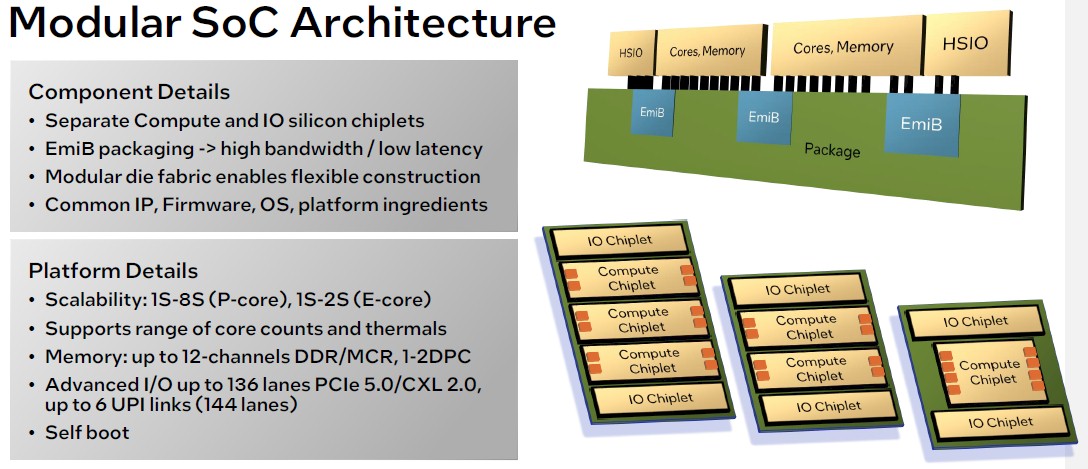
Intel is using its 2.5D Embedded Multi-die Interconnect Bridge (EMIB) multi-chip packaging technique to glue the chiplets together. EMIB is Intel’s answer to Taiwan Semiconductor Manufacturing Co’s Chip on Wafer on Substrate (CoWoS) 2.5D packaging, famously used for GPUs and other kinds of accelerators. Going forward, Intel could use its Foveros 3D chip packaging to add vertical L3 cache extensions to a Xeon SP design, much as AMD has done with its 3D-Vcache for its Milan-X and Genoa-X processors.
The chart above reflects the different options Intel has to build out chips in the 6th generation, but don’t assume that Granite Rapids and Sierra Forest will have all options as the SKU stacks are built out for both lines. Gianos says that, generally speaking, Intel will be able to offer Xeon SP chips with as low as single digit core counts and a pretty high amount of I/O using the designs on the lower right and scale up to triple digit core counts as you move to the chiplet packages on the left.
The E-core systems will support one to two sockets – meaning some of the UPI links will be disabled in the I/O dies – while the P-core systems will offer one, two, four, and eight sockets with a progressively larger number of UPI links activated. Each core chiplet will have four memory controllers, which will support DDR5 or MCR memory (more on this in a second), so the biggest 6th gen Xeon SP configurations will have twelve memory controllers serving their dies, with either one or two DIMMs per channel depending on the capacity and bandwidth needs of the customer. The pair of I/O dies will offer 144 lanes of UPI interconnect (that’s six ports, so three per I/O die) and 136 lanes of PCI-Express 5.0 interconnect (so 68 lanes per I/O die), and we reckon that half of those PCI-Express lanes will be able to support the CXL 2.0 memory protocol, although Intel could surprise us and make them all CXL 2.0 compatible.
With the 6th gen Xeon SPs, Intel is creating a kind of “virtual monolithic die,” as Gianos explains it, extending the on-chip mesh interconnect that has been used in Xeon E5/E7 and Xeon SP processors for more than a decade now across the EMIB interconnects. Any element of any chiplet can talk to any other element across this extended mesh just like it would do if the chip were monolithic, says Gianos, and there is over 1 TB/sec of bandwidth across those EMIB boundaries connecting the chipsets to make sure they can do it fast.
Gianos adds that in the Granite Rapids designs, there would be “over a half gigabyte” of last level cache on the top-end SKU, and says that Intel also says that it will also offer sub-NUMA clustering at the chiplet level as the default mode for allocating work across the chiplet and providing memory and compute locality.
Here is the compute die architecture for the 6th Gen Xeon SPs, using the Granite Rapids P-core variant as an example:
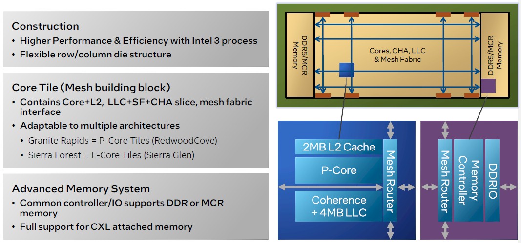
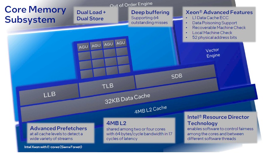
We know that the three chiplet, full sized E-core variant, Sierra Forest, has a maximum of 144 cores on a package with three chiplets. At 3 MB of LLC cache per core tile, where there are four E-cores in tile according to Soltis, that is 48 cores per chiplet and a dozen core tiles per chiplet, which works out to 36 MB of shared L3 cache per chiplet and 108 MB of shared L3 cache across the three-chiplet mesh with 144 cores. There is 4 MB of L2 cache dedicated to a four E-core tile, and with a dozen core tiles per chiplet, that 48 MB of L2 cache per chiplet and 144 MB of L2 cache per Sierra Forest package. (This is not the AP double up.) But not so fast. This might not be the right math.
With the P-cores, the math is a little different. There is a 4 MB of L3 cache segment per core and a dedicated 2 MB L2 cache segment for each core. To make a Granite Rapids, you pop out the quad of E-cores and their caches in the Sierra Forest compute chiplet and you pop in the P-core and its caches. With more than 512 MB of L3 cache, that implies that Granite Rapids can in theory have more than 128 cores per socket in the non-AP version. The P-core has HyperThreading at two threads per core, an AVX-512 vector unit, and an AMX matrix unit, so it is a much fatter core. This will be a much hotter chip than Sierra Forest, without question.
By the way, that 128 cores number does not quite jibe with something Soltis says in his presentation: “Conceptually, we remove the P-core and replace it with an E-core module,” Soltis says. “Everything outside of that are the same IP and you’ll see in a bit that we reuse the exact same silicon as well.”
Well, if you do that, then a Granite Rapids only tops out at 36 cores, which it can’t. That is not enough cores. So it could be that Granite Rapids has three tiles in the maximum configuration – that would be and Sierra Forest only needs two in its maximum configuration.
If this is the right scenario, each E-core chiplet might have 80 cores – in a 10 x 2 grid of four cores, perhaps. The yield might only be 90 percent on these chips so that could bust it down to 72 cores active, which would yield 18 active E-core tiles and 54 MB of shared L3 cache and 72 MB of L2 cache. Two of these would be 36 E-core tiles with 144 cores and 108 MB of shared L3 cache and 144 MB of L2 cache.
Now, take three of these, pop out the E-core tiles and pop in a P-core with 4 MB of shared L3 cache and 2 MB of L2 cache. At the full 20 core regions on a tile, that would be 60 cores, and let’s assume Intel will do deep bin searches and find versions that have all cores working. That still doesn’t sound like enough. Something still doesn’t add up, unless Intel is looking for an AP variant to double that again to 120 cores. Which we are beginning to think is the plan.
Just by gut, we think that 72 cores and 288 MB of L3 cache is the target top bin for the regular Granite Rapids chip, and a Granite Rapids-AP twofer would therefore have 144 cores and 576 MB of L3 cache – all across three chiplets. That fits the “greater than half gigabyte of LLC” that Gianos was talking about in his presentation. Work it backwards from there and you have an E-core chiplet that might have 84 cores in a grid and at 85 percent yield gives the 72 cores that we expect per chiplet based on what Intel has said about Sierra Forest. If that Sierra Forest uses only two compute chiplets. . . . Or, it is a 96 core part (perhaps with two chiplets) with a 75 percent yield to get to 72 cores.
Anyway, there’s a lot of ifs there. We know. The idea we need to focus on is this is the architecture and Intel can pull different levers and push different buttons to get to a desired end result based on how well or poorly its Intel 3 process, and the follow-on Intel 18A process that will be important for future Xeon SP chips, are doing. If the yields are bad, make the chiplets smaller and link more of them together.
Soltis said that there will be variants of the Sierra Forest devices that only have one core per pair activated. So some will top out at the same 72 cores, but with only 72 threads and presumably ones that are running at a higher clock speed and with slightly higher per-thread performance.
When asked about a rule of thumb to compare the P-core to the E-core, Gianos says that there really isn’t one. But we think the E-core will run at a lower clock speed and we expect for a P-core to have more than twice the single thread performance of the E-core pair. How much is debatable – 20 percent to 25 percent would not surprise us, which would generate a lot more heat than 20 percent to 25 percent more, especially with AVX-512 and AMX units on the P-core. But, for all we know, by stripping out these elements and going with a much thinner pair of 128-bit AVX vectors in the E-core, maybe Intel can run the clocks faster on E-cores than P-cores in the same thermal envelope.
We shall have to wait and see how this plays out.
Here is what the P-core looks like:
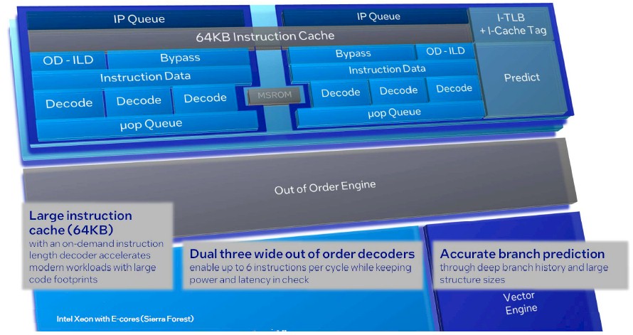
And here is what the E-core looks like:
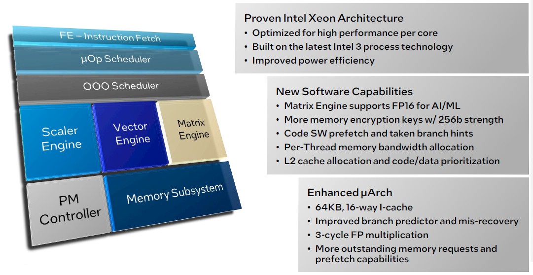
Both Sierra Forest and Granite Rapids are implemented in the Intel 3 process, which some say is like TSMC’s 5 nanometer process and others argue is more like its 3 nanometer processes. (Take your pick.) The important thing is that it is not a 10 nanometer process, or even a 7 nanometer process. Intel 3 is a good enough process shrink for Intel to compete with some additional architectural merits.
Both P-cores and E-cores have a 64 KB L1 instruction cache, which is important to keep the cores fed and, we think, is bigger to hide some of the inevitable latency that comes with using chiplets instead of a monolithic die design. Cache is king. . . .
Soltis drilled down a bit into the E-core architecture, which is the different one and which is known by the codename “Sierra Glen” inside Intel. (The P-core, codenamed “Redwood Cove,” is an update to the “Golden Cove” core used in the 4th Gen “Sapphire Rapids” Xeon SP processors shipping now.) Here is what the front-end looks like:
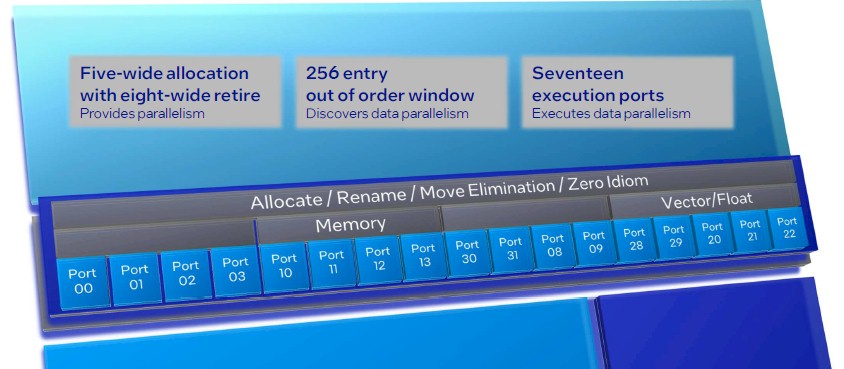
Here’s what the out of order engine unit looks like:
And here is what the execution unit looks like:
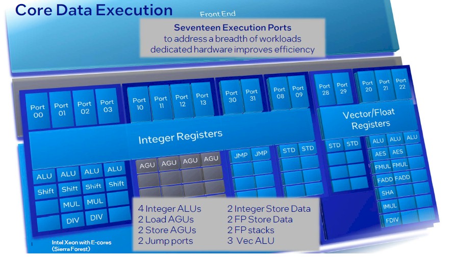
There is a reasonable balance of integer and vector performance, and Soltis said that the AVX unit in the E-core – not AVX-512 and not AVX-10 – would support INT8, BF16, and FP16 formats and presumably also FP32 and FP64, which he did not mention.
Here is the back-end of the E-core, down to the 32 KB L1 data cache and to the 4 MB of L2 cache that is shared across the two or four E-cores in a core tile:
The I/O die is the same for both Granite Rapids and Sierra Forest, which is why they can share the same platform.
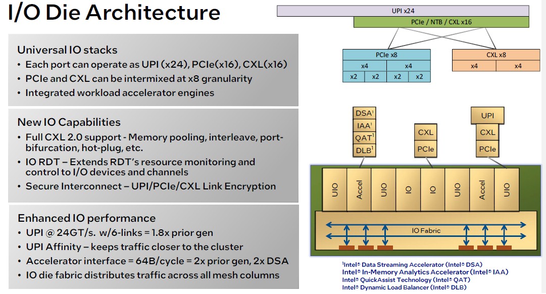
Intel is running the UPI links a little slower with the 6th Gen Xeon SPs, but they are also a little bit wider, too, and this is apparently balancing out the NUMA performance better than with prior Xeon SPs. The interfaces to the on-chip accelerators is also twice as wide to boost their efficiency as they are running.


Great to see Intel stepping back into the ring of the competitive no-holds-barred datacenter rumble with AMD, Ampere, and NVIDIA, who seem to have had just too easy a time of it lately! 144 P-cores of AP Granite sounds like a Dwayne-Johnson rock-solid ticket for this show!
Speaking of which, with chiplets ahoy, and copy-paste gods-of-the-Neoverse Cascading-Style-Sheets (CSS), it should be but a walk in the Zen monastery’s park for AMD to shimmy itself together (duct-tape? nope) an enlightened MI300N AI/ML Buddha, with 96 ARMs and 4 basic Instincts … less Seattle, more Shaolin!
A 288-ARM Buddha (6 x 48-core-dies) might even have the computational guts to meet the E-cores, behind the announced Sierra-Forest, for an explanation on perf/watt (or not?)!
Will IBM’s heroic POWER10 ever stop sulking and rise back to the challenge? Who will be the suplexest of them all? “Inquisition minds” … (as Lechat once said!).
It’s (mildly?) interesting that there isn’t a lot of international competitors for this rumble, maybe just A64FX.
It makes one wonder what the status of the EU’s SiPearl Rhea (72x Neoverse V1, 2x256b vectors) might be, whether it might be paired with Barcelona’s MEEP ACME self-hosted RISC-V-based accelerators (MareNostrum Experimental Exascale Platform’s Accelerated Compute and Memory Engine), and/or if their derivatives might find datacenter applications.
Also, although the Phytium/Matrix-2000+ (FTP/MTP) 64x armv8 cores paired with 128x matrix units is presumably seeing field use in Tianhe-3, and the SW26010Pro that pairs a single “proper” CPU (MPE) with 64x 256-bit “vector” cores (CPEs) (in groups of 6) is running in OceanLight, their 14nm process (?) seems to set their usable performance behind that of competitors. SMIC’s DUV N+1 7nm would be ok for efficiency (eg. Huawei smartphones) but not so much for performance (where EUV would be needed). It could be a good thing or a bad thing, depending on one’s perspiration …
My-oh-my … MEEP meep (The Road Runner?) and ACME (Wile E. Coyote?) … what could possibly go wrong??? Major cliffhanging, delayed-gravity, anvil dropping, painted tunnel-entrance, EuroHPC entertainment … straight ahead!!!
Yep, and depending on which way your sweat mostly leans, you might need extra-antiperspirant (or not) when considering the IO500 storage subsystem performance results (https://io500.org/), where Pencheng (Tsinghua) and JNIST/HUST (Huawei) blow the competition straight out of the drip-pan!
I like those 17 execution ports of Sierra Glen, numbered 00 to 31, leaving room for 15 more (or different mixes) in future updates! Also, 64 KB of L1 I-cache is right on the money, but 32 KB for D-cache looks a bit low to me (64 KB could be more competitive I think, if it fits). Support for channel-doubling MCR DIMMs is definitely great (my interpretation of MCR). And there seems to be CXL 2.0 support in the I/O die hardware (last slide), possibly some protocolar IP aimed at simplifying channel setup and management (the slide mentions hot-plug)? Not to mention Intel In-Memory Analytics Accelerator (IAA) for database workloads (but what does it do, really?).
All-in-all a quite interesting DC chip — not sure what I’d want to add to it (except more L1 D-cache)!
I think of MCR as like PAM4 for memory. Not literally, but effectively. It’s not really doubling the channels but multiplexing the transport for the channels and boosting the gain.
I’m going to do a separate piece on MCR.
That the E cores run at lower clocks due to thermal limits, yet the entire industry calls them “Efficient” is a testament to Intel’s greatest strength: marketing.