

Innovation requires motivation, and there is nothing quite like a competitor trying to eat your lunch to wake you up every morning to the reality of the situation. From a financial standpoint, the decline of the RISC/Unix vendors and the absence of AMD from the server market was great for Intel, and its hegemony in the datacenter has never been greater and its revenues and profits continue to break records.
That latter bit is a lucky break caused by the rise of the hyperscalers and cloud builders, who have provided some of the competitive pressures that would have normally been placed on Intel by direct competitors and OEM and ODM partners who play off suppliers. While Intel has been fortunate in increasing its near monopoly on compute servers in the datacenter and expanded out to networking (with limited success) and storage devices (with much better success with flash memory and thus far delayed and iffy results with Optane 3D XPoint persistent memory), the lack of competition has really hurt Intel’s engineering edge.
It’s a good thing for Intel that it is making money hand over fist, and that the server market is growing faster than its much smaller rivals can eat market share, so the AMD Epyc and Marvell ThunderX2 assaults and some sword waving by IBM Power9 have not really dented Intel’s core server business. And the two-year delay of 10 nanometer processes, which has made a mess of Intel’s roadmaps, has not really had an impact. But in 2019, as AMD and Marvell ramp their next-generation devices on advanced processes from Taiwan Semiconductor Manufacturing Corp, the heat will be coming to Intel and it very likely will be burned.
It is the job of Raja Koduri, senior vice president of the Core and Visual Computing Group, general manager of edge computing solutions and chief architect at Intel, and Jim Keller, senior vice president of silicon engineering, to blunt the attack. Koduri and Keller are the people responsible for AMD’s resurgent Radeon GPU and Epyc CPU lines, respectively. And these two, among other top brass at Intel, laid out the plan of attack and defense at an Architecture Day event hosted this week at the former mountain estate of Intel co-founder Robert Noyce in Los Altos. A fitting scene as Intel looks down from on high on Silicon Valley and tries to carve out an even bigger piece of real estate for itself in the datacenter.
Rome Wasn’t Built – Or Sacked – In A Day
We are going to get into the finer details about what was said at Architecture Day, the conversations we had with both Koduri and Keller, and what we think in response to what was revealed, but in this initial piece we will just take the high level view that the two presented to kick off the day.
Everyone is familiar with the tick-tock methodology that Intel employed for more than a decade, which was famously crafted by Pat Gelsinger, formerly the head of Intel’s Data Center Group and once the heir apparent at the chip maker but who was passed over for the chief executive officer job and therefore who left to become the top executive at VMware. With the tick-tock method, Intel breaks the chip refinement process into two parts to mitigate against risks, with a tick being a transistor manufacturing process shrink and a tock being an architecture change that makes use of that process perhaps 12 to 18 months later after it has been refined and ramped. With the tick-tock method, Intel could keep a steady stream of performance improvements coming, and it worked really well. Right up to the point where the ticks were taking longer and the tocks were getting harder.
Intel broke with the tick-tock method starting with 14 nanometers, extending its life and making it tick-tick-tick-tick to squeeze more and more performance out of that chip making node – something that was necessary thanks to the delay in the rollout of 10 nanometer manufacturing processes, which as our colleague Chris Williams over at The Register points out, Intel was five years ago confident it could get out the door in 2015, then 2016, then late 2017, then late 2019, and now, at least for servers, early 2020 when the “Ice Lake” Xeons debut. This has caused a stretching tick at 14 nanometers and a slipping tick at 10 nanometers and a whole bunch of smushed up tocks that were dependent on the 10 nanometer process.
The lesson, it seems, is to not have your tocks so dependent on the prior ticks, and to learn to mix and match chip elements etched in different processes and jam them into a 2D package or stack them into a 3D package. In effect, you only push the tick on the bits of the chip where that will help and you leave the rest of the chiplets that go on the package – such as memory controllers and I/O controllers that have to use lots of power to go off chip – in mature transistor etching processes that are bigger, but a lot cheaper to manufacture. This is what AMD is doing with its future “Rome” Epyc CPUs, what Barefoot Networks is doing with its future “Tofino 2” switch ASICs, and what Xilinx is doing with its “Everest” Versal FPGAs. (By the way, all three of those chips, due in volume in 2019, are using the 7 nanometer processes from Taiwan Semiconductor Manufacturing Corp for the core compute elements of their products, with other chiplets on the package being etched in older and more mature 16 nanometer or 12 nanometer processes.)
This was Architecture Day, not Manufacturing Day, at the Intel event – a discussion of tocks more than ticks, as it were – but the two are increasingly related while at the same time less dependent on each other, strangely enough. So Intel did not talk specifically and broadly about how future Atom, Core, and Xeon processors would be comprised of chiplets based different etching sizes, but this is what was strongly hinted at by Koduri, who said in his opening keynote that Intel was far too dependent on its transistor shrinks and architecture tweaks, and that since joining Intel a year ago after a sabbatical from 25 years of chip design, he has come to the conclusion that Intel not only needs to redefine its goals, but also rely upon more levers than these two – process and architecture – to accelerate the company’s business.
But one note about process that is important. One thing that Intel did learn is that when pressed, it can squeeze a lot more performance out of an existing process than perhaps it thought it could, and the current 14 nanometer FinFET process etching its Core desktop processors is a good example, and one that could be applied to Atom chips or Xeon chips for servers, too. Here is a chart that shows the evolution of top clock speeds in the Core chip lineup in the past several years as the processes were refined:
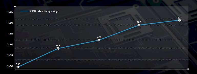
The baseline 4.2 GHz in the chart above is the top clock speed of a “Broadwell” Core chip etched in the first pass of the 14 nanometer process, followed by a “Skylake” part, which had a 7.1 percent boost in clock speed to 4.5 GHz due just to the refinement in the process. With the “Kaby Lake” follow-on to Skylake, which never made it into Xeon SP servers, there was another 4.4 percent increase in clock speed to 4.7 GHz, and with “Coffee Lake” chips on a further refined 14 nanometer process, the clock speeds jumped another 6.4 percent to 5 GHz, and a further refinement of Coffee Lake chips on an even better 14 nanometer process pushed that up a tiny bit more to 5.1 GHz. If you do the delta across the five Core chip generations, that is a cumulative 21.4 percent increase in the maximum clock speed just from process refinement – almost as much clock speed increases as Intel can push when it changes a full process node. So maybe a smoother refinement is the name of the game, making each process node last longer even as new ones come around.
This smoother approach could help alleviate some competitive pressures, but Intel ramped down its 14 nanometer equipment and ramped up its 10 nanometer gear before it was ready, and that has caused shortages of PC chips and some server chips in 2018, forcing Intel to concentrate its best yielding and best performing 14 nanometer processes on the highest performing PC and server parts it puts out.
This tick-tick-tick-tick-tick methodology is something that Intel needs to get customers used to, and it will change the way it ramps up and ramps down gear in its factories to meet demand.
The main thing that Koduri wanted to make sure everyone understood is that Intel now has its 10 nanometer situation under control, and that it is looking ahead to 7 nanometers and beyond, presumably to 5 nanometers, in the coming years. Here is what the current path looks like:
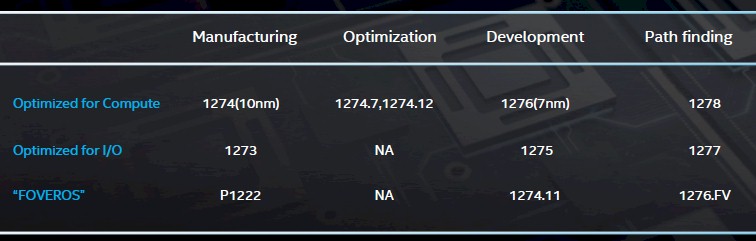
As you can see, Intel has two different versions of each node – one optimized for compute and the other for I/O, which require different properties from the transistors that Intel etches with each process. Processes variants ending in even numbers are for compute and those ending in odd numbers are for I/O, and at the initial revised 10 nanometer node, the variant that is in manufacturing today – meaning it is being used to create chips – is called 1274, and the I/O version is called 1273. In the chart above, Foveros refers to the 3D chip packaging technique that Intel has created for an unnamed customer to mix Core and Atom processors on the same package, stacked on top of each other and linked to each other and other components on the package (more on this in a moment).
After the initial 10 nanometer process, there are two nodes in compute that are being created as optimizations – what Intel might have called 10 nanometer+ and 10 nanometer++ a few years back to the outside world; these are known as 1274.7 and 1274.12 internally. There is no optimized variant for chips that are heavy on the I/O. Concurrent with this, follow-on 7 nanometer processes – 1276 for chips aimed primarily at compute and 1275 optimized for chips that are heavy on the I/O – are in development, and further out Intel is doing “pathfinding” research on the 5 nanometer processes, known as 1278 and 1277 for compute and I/O SKUs, respectively.
The point is, Intel is still a chip manufacturer and it is still working very hard on getting its nanometer shrinks in order and coming to market with ever-better transistors.
A Plethora Of Processing
But there is a larger problem that needs to be addressed, and that is the Cambrian explosion in types of compute in the datacenter. Intel has been building up a portfolio of different kinds of compute, and it knows full well that it needs to add discrete GPUs that can be used as accelerators alongside its Xeon and Atom server CPUs, its Arria and Stratix FPGAs (from its Altera acquisition), and its Crest neural network processors (from its Nervana acquisition). Intel needs something to directly compete against Nvidia Tesla and AMD Radeon Instinct GPU accelerators, and that is one of the reasons why it hired Koduri in the first place.
It is not so clear how Intel is going to help customers choose what kind of compute to use for any particular workloads, since there will be substantial overlap in many cases.
But before we go down that rabbit hole, let’s take a step back for a minute before we get into all of these chip mixes. Intel has said time and again that it is no longer chasing a $45 billion total addressable market for client and server processors with some flash memory and occasionally some interconnect thrown in, and that it is rather pursuing a much broader $300 billion market, embedding itself in all manner of gear in the datacenter, on the campus, and at the edge. Paying for all of that chip research and foundry building, Intel is going to have to make it up in volume.
The first thing that Koduri reminded everyone was that not all transistors are good at everything, and that as a diverse supplier of electronics dealing in a world where Moore’s Law is slowing, different kinds of circuits require different process technologies. Even if you could create monolithic system on chips doing a plethora of things using a single process, maybe that is not the smart thing.
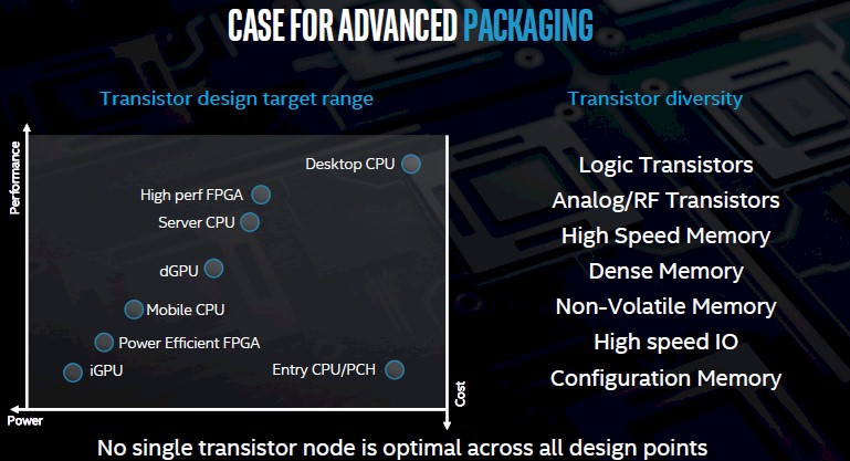
“With our ambition to build a $300 billion TAM, and entering different markets, one thing that we noticed is that the design range for the transistors we need to build is huge,” explained Koduri. “A desktop CPU, for example, is at one end of the performance/power spectrum, and a new transistor is not always the better transistor across these uses. And actually, there is no transistor that covers all of these targets. Also, the diversity of transistors that we need to integrate is increasing – we have comms transistors, I/O transistors, FPGA transistors, as well as the classic CPU logic transistors.”
This is true within monolithic chips that need to be broken down into chiplets for economic and technical reasons as well as across different markets where different pieces need to be integrated in different ways for various power envelopes, performance profiles, features, and costs. Everything in the industry pointing toward multichip packaging inside of a socket, and not just at Intel, as we have noted.
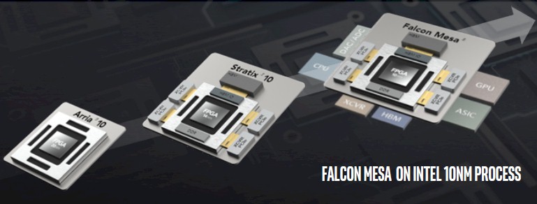
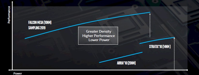
And so, that is what Intel is going to do. Exactly when and with what circuits is not clear, but clearly it is using a modular socket design with the future “Falcon Mesa” FPGAs coming out of its Programmable Solutions Group, which will be using 10 nanometer processes for at least the core logic:
The chiplet approach is not just about making a part with different components tuned to the right process, but being able to make a collection of parts that fit a wider performance and power profile than can be done with a monolithic chip. Take a look:
This is all implied from Koduri’s talk, not specifically and precisely roadmapped, mind you.
Another component coming on 10 nanometer processes – and perhaps not shrinking again for quite some time into the future – are Intel’s 112 Gb/sec SerDes circuits, which support pulse amplitude modulation to pack more bits into a signal. To be precise, they support PAM-4, which allows for four layers of signaling (or two bits) to be encoded at the same time, which is double the bit rate of the non-zero return, or NRZ, encoding that has been used to date. After the forward error correction and encoding overhead is taken into account, that means the 112 Gb/sec SerDes that Intel has created in the labs can deliver 100 Gb/sec native per lane. The lanes actually run at a net 50 GHz and the PAM-4 gets you two bits per signal, for an effective 100 Gb/sec, and then you add up the lanes to get the bandwidth you want on a server or switch port, ranging from 100 Gb/sec for one lane to 800 Gb/sec for eight lanes.
![]()
The fact that Intel has 112 Gb/sec SerDes means that Intel is on par with the industry for both Omni-Path 200 and Ethernet connectivity, which is necessary for the company to compete against its many networking rivals, many of whom are also trying to sell processors against Intel in one fashion or another.
That brings us to the Foveros 3D chip packaging effort, which is blazing the trail for how compute engines from Intel will be architected in the not-too-distant future. Foveros, which is a system-in-package integration, adds a second dimension to the Embedded Multi-die Interconnect Bridge (EMIB) multi-chip packaging technique that Intel has talked about as a research effort for years and that was actually implemented on the Stratix 10 FPGA to interconnect chiplets and on the Intel Kaby Lake-G Core chip equipped with AMD GPUs and High Bandwidth Memory (HBM) on a single package.
With Foveros system-in-package multi-chip modules, the I/O circuits, SRAM caches, and power circuits that serve the compute complex (which can include memory and other components) are made on a base die, which sits atop the package substrate that in turn has the pins that mate to a socket or that get welded directly onto a motherboard. An active interposer is placed atop this package substrate, which has through-silicon vias (TSVs) linking different kinds of chiplets to each other over this interposer. The chiplets have micro-bumps that link them to the TSVs and down into the interposer and therefore to the chips on the bottom of the stack and across the interposer to other chips that are adjacent or stacked on top. You can have a layer of bottom chips and then another layer of top chips. There is a lot of layering going on:
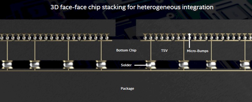
Look at how shiny those solder bumps look; this is what happens when a graphics guru does a presentation.
The first product using the Foveros approach was demoed at the Architecture Day event, and it looks like this:
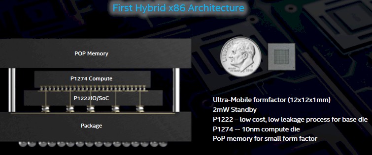
This particular device is aimed at ultra-mobile uses, and the package is, at 12 millimeters by 12 millimeters, much smaller than a US dime. The base die which has the I/O and other system-on-chip components is implemented in the 1222 process, which is code for the base 22 nanometer process that has long since been perfected and showed up in the Xeons in the “Ivy Bridge” and “Haswell” generations. Again, larger transistors are better for power and I/O circuits. On top of that is a compute complex implemented in the 10 nanometer process (1274, with a P in front to designate a Foveros stacking), and in this case, it includes a single core from the “Sunny Cove” Core generation and four cores from the “Tremont’ Atom generation, in the hybrid fashion that the Arm collective has been using for years. On top of that is a chunk of package-on-package (POP) main memory. Intel did not say what the power draw would be of this chip complex under load, but did say that it would draw 2 milliwatts in standby, which is about as low as you can get.
Intel has not said if it will be using Foveros techniques in future Core and Xeon processors – and that term is going to get a lot more slippery going forward – but it is clearly going to be using them in the future “Falcon Mesa” FPGAs as well as in its future Xe discrete GPUs, coming in 2020. And we suspect, also in the future Xeons, Atoms, and hybrids that mix and match various CPUs with GPUs, FPGAs, and other things like the Nervana neural network processors on a single package.
The key message is that Intel is not just relying on process and architecture (with packaging being part of architecture) to drive its compute business, but will make full use of its memory and interconnect chips, and embed security into all elements and unit them with a less complex, integrated collection of software that spans all of these different compute elements, which it is calling oneAPI. We will be drilling down into oneAPI as well as roadmaps for the various compute engines and their expected effect on getting back on the Moore’s Law track separately. Stay tuned.

What Would You Do With A 16.8 Million Core Graph Processing Beast?
If you look back at it now, especially with the advent of massively parallel computing on GPUs, maybe the techies at Tera Computing and then Cray had the right idea with their “ThreadStorm” massively threaded processors and high bandwidth interconnects. Given that many of the neural networks that are created …
The Next – And More Profitable – 10 Percent Of Server Share For AMD
When this is all said and done, Intel will deserve some kind of award for keeping its 14 nanometer processes moving along enough as it gets its 10 nanometer and 7 nanometer processes knocked together to still, somehow, manage to retain dominant market share in the server space. Or, maybe …
Building A Better Machine For An AI World
Raja Koduri has been in the thick of the past two eras of computing, which were marked by – among other things – the ability to architect systems and software that helped to get more performance into the hands into increasing numbers of people. In two stints with AMD, Koduri …
dont you love how the machine works though
Wow! They are desperate… they need sell this crazy stuff to show they are better than the competition… they lost their advantage already. AMD, ARM, IBM coming back! Finally, some real competition!