

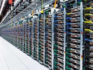
The gap between the performance of processors, broadly defined, and the performance of DRAM main memory, also broadly defined, has been an issue for at least three decades when the gap really started to open up. And giving absolute credit where credit is due, the hardware and software engineers that created the cache hierarchy and the software that could take advantage of it have been nothing short of brilliant. This is some of the hairiest architecture that has ever been devised by humans.
But as we sit at the cusp of an ever-expanding memory hierarchy as persistent memories like Optane 3D XPoint (a variant of phase change memory) come to DIMM and SSD form factors and new protocols like CXL, OpenCAPI, CCIX, NVLink, and Gen-Z are being introduced to link processor and accelerator memories coherently together (either symmetrically or asymmetrically), we got to thinking: Is it time yet to add Level 4 caches to servers? With so many different devices hanging off the CPU complex – some relatively close and some relatively distant – it is logical to wonder if another cache level will be necessary to mask latencies of these other memories and boost overall system throughput.
To get a sense of what might be possible, we poked around in our own memories and also reached out to the server chip architects at IBM, Intel, AMD, and Marvell to get a sense of what they thought about the use of L4 cache memory in servers. L4 cache is by no means a new development, but it is also not commonplace in system architectures.
But before we get into that, a little background is in order.
The addition of Level 1 caches to processors, which only had one core way back then, in the late 1980s made a tradeoff between adding overall latency to the memory subsystem in exchange for absolutely lowering the overall average latency for data and instruction requests by the processors. L1 caches were originally external SRAMs that were mounted on motherboards and wired into the CPU-memory complex. This L1 cache sat very close, in both clock time and motherboard space, to the processor, and meant that the CPU could be kept busier than might otherwise have been possible. Eventually, these Level 1 caches were split so they could store frequently used data in one chunk and popular instructions in another, which help boost performance a bit. At some point, as processor clock speeds increased and the gap between CPU speed and DRAM speed opened up even further, fatter but slower and cheaper (on a per bit or per bandwidth basis) L2 caches were added to the mix, again first outside the CPU package and then integrated on it. And when more and more cores were added to the CPU as well as more DRAM memory controllers to feed them, even bigger blocks of L3 cache were added to the hierarchy to keep those CPUs fed.
This has, for the most part, worked out pretty well. And there are some rules of thumb that we see in most CPU designs that reflect the levels of cache hierarchy in processing as we contemplate a possible fourth.
Chris Gianos, the chip engineer and architect at Intel who has led the design of many of the past generations of Xeon processors, explained it like this: “With each cache level, usually we need to grow them by a reasonable amount over the previous level to have it makes sense because you need an interesting enough hit rate to actually make a notable effect on your system performance. If you are only hitting the cache a few percent of the time, it’s probably going to be hard to notice. Everything else is swamping your performance and you haven’t moved the needle too much. So you need relatively big caches, and when you’re talking about the higher levels, you need really big ones. These days our L2s are measured in megabytes and our L3s are measured in tens or hundreds of megabytes. So clearly, if you start thinking about an L4 cache, you are probably in the hundreds of megabytes if not gigabytes. And because they are big, their cost is definitely a concern. You’ve got to put enough down to make it interesting and it won’t come cheap.”
The architects at AMD, who did not want to be directly attributed because in having this conversation they did not want to be misconstrued with AMD promising that it would be adding L4 cache to the Epyc processor line – and to be clear, AMD has said nothing of the kind. But it did recognize that it is the next obvious thing to be thinking about, and just like Intel, believes that every architect is thinking about L4 caches, and it shared some of its thinking on background. Basically, AMD says that the tradeoff in number of cache layers and latency has been well studied in industry and academia, and that with each new cache layer, which is bigger, slower, and more widely accessed, there is a necessary tradeoff that increases the total path out to the DRAM because most designs would not continually speculatively access the cache layers further down in the hierarchy in parallel with cache tag lookup in the upper layers. This is exactly what Intel is also talking about above when Gianos says you need to find a balance between the hit rate and the capacity of the cache – and the L4 is no different.
IBM, of course, added L4 cache to some of its own X86 chipsets back in the 2000s, and in 2010 it added L4 cache to the NUMA interconnect chipsets on its System z11 mainframes. The z11 processor had four cores, each with 64 KB of L1 instruction and 128 KB of L1 data cache, plus 1.5 MB of L2 cache per core and a 24 MB shared L3 cache across those four cores. The NUMA chipset for the z10 had two banks of 96 MB of L4 cache, for a total of 192 MB. With the z12, IBM cut back the data cache to 98 KB per core but boosted the L2 cache per core to 2 MB while splitting it into instruction and data halves like the L1 cache; the L3 cache was doubled up to 48 MB across the six cores on the die, and the L4 cache capacity was increased to 384 MB for the pair of chips implemented on the NUMA chipset. On through the System z processor generations, the caches have all grown, and with the z15 processor announced last September, the pair of L1 caches weigh in at 128 KB each, the pair of L2 caches weigh in at 4 MB each, and the shared L3 cache across the 12 cores on the die comes in at 256 MB. The L4 cache in a drawer of z15 mainframe motors has 960 MB of L4 cache in the NUMA chipset and a total of 4.68 GB across a five drawer complete system that scales to 190 cores.
As we have pointed out before, the Power8 and Power9 processors both had buffered memory and IBM added a chunk of 16 MB of L4 cache memory to each “Centaur” buffer, for a total of 128 MB of L4 cache per socket across 32 memory sticks. With the Power9, the low-end machines don’t have buffered memory and therefore do not have L4 cache. The architects who are did the Power10 designs and are doing the Power11 designs were on deadline this week and could not hop on the phone, but William Starke, who steered the Power10, effort, spared a little time anyway to add this thought to the mix:
“In general, we have found that large last-level caches provide significant performance value for enterprise workloads,” Starke explained to The Next Platform by email. (We talked to Starke back in August 2019 about cranking up the bandwidth on the main memory complex with the Power9 and Power10 chips. “Separately, the high latency associated with persistent storage technologies such as phase-change-memory tends to drive a strong need for caching – possibly L4-like – in the storage class memory hierarchy.”
This was precisely our thinking. And by the way, we are not suggesting that the L4 cache will necessarily sit on or next to the buffered memory on the future DDR5 DIMM. It may be better suited between the PCI-Express and L3 cache on the processor, or maybe better still, in the memory buffers and between the PCI-Express bus and L3 cache. This might mean stacking it up on top of the I/O and memory controller hub chip in a future chiplet server architecture with something akin to Intel’s Foveros technology.
Now, to be fair, there is another way to look at this, and that is that IBM had die size and transistors to play with, and adding L4 cache to the System z NUMA interconnect or to the Power8 and Power9 memory buffer chip was not precisely the goal in and of itself, but the best thing to do with the leftover transistor budget available on these devices once the other required features were added. We sometimes think that cores counts on Intel X86 processors are opportunistic relative to the amount of L3 cache that can be laid down. It sometimes looks like Intel sets an L3 cache budget per die and then it all falls into place for three different sized Xeon dies – in recent generations, those with 10, 18, or 28 cores, as it turns out on 14 nanometer processes.
Al of this is moot, but it suggests a possible motivation that IBM and other chipset makers have had for adding L4 cache. Not only could it help some, but it was something obvious to try. We think on such an I/O monster as the System z mainframe, there is no question that IBM has the L4 cache right where it works best and it brings value to customers by increasing the throughput of these machines and allowing them to run at a sustained 98 percent to 99 percent CPU utilization as the processor core counts and NUMA scale have both risen in mainframes.
Chew on those percentages for a second the next time you hear the word “mainframe” in a sci-fi show. (I have a drink each time I do, and it’s a fun game if you binge watch a lot of different sci-fi shows in a row. Nobody ever says: “The distributed computing system is down. . . .” Past, present, or future.)
There is no reason why L4 cache has to be made of embedded DRAM (as IBM does with its chips) or much more expensive SRAM, and Rabin Sugumar, a chip architect at Cray Research, Sun Microsystems, Oracle, Broadcom, Cavium, and Marvell, reminds us of this
“Our L3s are already quite big as far as that goes,” says Sugumar. “So an L4 cache has to be made in a different technology for this particular use case that you are talking about. Maybe eDRAM or even HBM or DRAM. In that context, one L4 cache implementation that seems interesting is using HBM as a cache, and that is not a latency cache as so much as a bandwidth cache. The idea is that since the HBM capacity is limited and the bandwidth is high, we could get some performance gains – and we do see significant gains on bandwidth limited use cases.” Sugumar adds that for a number of applications, there are a relatively high number of cache misses. But the math that needs to be done – both for performance and for cost – is if adding another cache layer will be worth it.
(And once again, Sugumar talking to us about this does not mean that Marvell is committing to adding L4 cache to future ThunderX processors. But what it does mean is that architects and engineers always try out ideas – usually with simulators – long before they get etched into the transistors.)
One possible other L4-like caching option, says Sugumar, is to use local DRAM as a cache. “This is not in the development lab or anything like that, but let’s say we have a high bandwidth interface on our chip that’s going to a shared distributed memory somewhere on the other end of the wire that is between 500 nanoseconds to a microsecond away. Then one usage model would be to create a cache that moves this data from shared distributed DRAM to local DRAM. We can imagine running a hardware state machine that manages the memory, so most of the time it takes the local DRAM and you minimize the number of times you go out to shared DRAM.”
This sounds like a funky kind of NUMA to us. By the way, Sugumar worked on distributed memory for high-end parallel systems at Sun Microsystems, and this was before persistent memory was available. And the one concern of having these various memory hierarchies was that if one of them gets lost from a network or interconnect failure, then the whole machine comes down – boom! “You have to deal with network failures in distributed memory systems in a more graceful manner, and that creates a lot of challenges in the design.”
The other thing is that we want any higher level cache, even if it is not an L4 cache, to be implemented as much in hardware as possible and with as little software tuning and application change as possible. It takes a while for operating system kernels and systems software to catch up to hardware, whether it is adding cores or L3 or L4 caches or addressable persistent memory.
“At some level, another level of cache is inevitable,” says Gianos. “We had a first level of cache and eventually we had a second. And eventually we added a third. And eventually we will have a fourth. It’s more of a question of when and why. And I think your observation that there is a lot of opportunity out there is good. But, you know, Intel hasn’t made a determination of exactly when or why that we are willing to publicize. Other companies are looking at it; they would be foolish not to think about it. It will happen sooner or later, but whether or not that is near term or further out, we’ll have to see.”

Vertically Unchallenged
Components make compute and storage servers, and servers with application plane, control plane, and data plane software running atop them or alongside them make systems, and workflows across systems make platforms. The end state goal of any system architect is really creating a platform. If you don’t have an integrated …

Talking System Architecture With AMD CTO Mark Papermaster
It is funny to think that in a certain light, AMD has Big Blue to thank for its resurgence in the datacenter. And not because IBM is not good at crafting processors and interconnects, but because some of the seasoned executives who honed their skills in semiconductors at IBM ended …
Making Sure AMD Has The Complete Tech Package
The chief technology officers in the tech world have done their time in the engineering trenches, writing their papers, getting their patents, and helping suppliers up and down the IT supply chain make the money that keeps the innovation flowing. But someone always needs to focus the imagination and enthusiasm …
The architects at AMD appear have redesigned their per CCD Die L3 cache layout with the Zen-3 based CCD getting rid of the CCX unit construct and having the Zen-3 CCD’s 8 Zen-3 cores share the entire CCD’s allotment of L3. So as far as Epyc/Milan is concerned it’s only a question of if the per CCD total L3 cache allotment will be made even larger compared to Zen-2’s per CCD Die L3 cache allotment. That removal of the 2, 4 core CCX units per CCD in favor of the just an 8 core CCD that shares all the L3 on the CCD has eliminated one Infinity Fabric domain level on Zen-3 and will cut out the intra-CCD(CCX Unit) Infinity Fabric latency hop that occurs on Zen-2 and Zen-1 when some L3 Cache line resides on the other CCX unit’s L3. And on Zen-2 everything IF based get routed via the I/O die, and ditto for Zen-3.
Maybe L4 can be figured in on Zen-3 or Zen-4’s I/O die once that I/O Die production moves to a 7nm/smaller process node but for Zen-3 there is no news on if AMD will want to shift the I/O die production below 12nm what with Global-Foundries’ 12nm node allowing AMD to keep its limited TSMC 7nm production capacity available for Zen-2’s and Zen-3’s 7nm based CCD production and 7nm Radeon GPUs.
Maybe after Apple shifts its A series production to TSMC’s 5nm node that should free up more TSMC 7nm wafer starts capacity for AMD but maybe it would be better spent on enlarging Zen-4’s per CCD L3 cache allotment. It all depends on what’s the better option more 7nm CCD’s per wafer and maybe some L4 cache on that 12nm I/O die or larger per CCD L3 cache allotments on 7nm/7nm+ and some CCD that’s a little bigger with less CCDs per 7nm/7nm+ wafer produced.
Great post. If zen3 skips that inter ccx data hop on the cdx, I can see where the “like a new gen” improvements are coming from.
L4 does exist, it is called M.2
The only thing standing in the way is that most hardware architectures are targeted by Java.
It wouldn’t matter if you had a terabyte of L1, Java would just garbage collect.
With Intel’s speculative flaws, the NSA’s relentless power, and Java’s horrible use of memory combined – will give rise to the steaming pile of garbage called an Intel product.
@Ken: M.2 is a slot (form-factor), not a type of memory. Further, you can’t have L4 cache that’s supposed to be faster than DRAM made out of SSDs. I don’t see how SSDs could ever become faster than DRAM on current technology.
If IBM stills sells big-iron with more than 4 sockets, then they want big cache to hide long memory latency, both in hops, and the complex NUMA system. In Intel world, most people have given up on 8-socket, and many probably realize even 4S is overkill.
Of course, I am of the opinion we should go single-die singe-socket for lowest possible memory latency, then push DRAM vendors to make low-latency DRAM as main memory in 1S systems.
Intel also needs to rethink the long latency of L3 cache, 19ns for the 28c Skylake. If that is how long it takes to check all caches on a very large die, then there is nothing we can do on that front. But, if we have low latency, fast turn-around memory, the we should issue the L3 and memory access simultaneously (note, one purpose of shared L3 is to help maintain cache coherency).
Each level of cache has a purpose/objectives. L1 needs to be very close and hence cannot be large. Even though it is 4-cycle, those are built into the processor-core pipeline. L1 instruction and data are separate because they are used by functional units in different locations of the core. L2 is there to make up for the L1 being too small, while still being reasonably low latency, at 3-4ns (12/14 cycles).
Years ago (2002-09), Intel had Xeon (MP) and Itanium processors with giant cache, in terms of percentage of the overall die. That doesn’t happen anymore because it is better to cram more cores on to the, only having L2/L3 to maintain cache-coherency and not overwhelm the memory channels.
It’s natural to think of solving cache limitations with a hardware solution, because most of us consider it a hardware problem. But the number of software cache levels in the hierarchy is not fixed by hardware. Indeed, this is truly self-evident when one considers that hardware might have three levels of cache, but a modern operating system might manage its own set of caches—for example, to store pages of memory or blocks of disk storage. Further, a SQL database might have its own set of caches used for its own purposes, such as storing indices, recovery data, or other data it sees being retrieved or
updated on a frequent basis.
Cache, then, is more flexible than silicon alone would have us believe. And this leaves room for one to make the argument that by intelligently increasing the cache hierarchy, one could also increase overall performance. Further, by doing it in software, one is not bound by the traditional limitations of silicon footprint and the traditional physical
constraints of power and heat dissipation.
Software-Defined Servers do this already—in effect delivering an L4 cache by utilizing a cache-only design. This is achieved by aggregating the resources (DRAM, cores and I/O) of multiple server systems into a single virtual system comprised of guest processors and guest virtual memory. These guest resources become operational by
mapping them to real physical processors and real physical memory as needed, on a demand-driven basis.
I’ve just posted a blog that explains how this works—and how extending the hierarchy further (L5 cache, anyone?) doesn’t have to be just another whiteboard discussion.
Read the blog here: https://blog.tidalscale.com/cache-is-indeed-king
IMHO, just as cache compensates for the data hops, there seems a ove in some apps like ai training, to remove hops by processing at the edge (& counter the transmissin costs of huge data).
NVME controllers w/ limited compute power e.g. could reduce transmissions to the center?
Sometimes it goes the other direction.
Cerebras has 18 Gigabytes on chip memory / 400000 cores = 45 kilobytes per core.