

If memory bandwidth is holding back the performance of some of your applications, and there is something that you can do about it other than to just suffer. You can tune the CPU core to memory bandwidth ratios by picking your chips wisely, and you can lean on chip makers and system builders to push it even further.
It is interesting to contemplate what HPC and AI computing might look like if CPUs were not so limited on memory bandwidth and in some cases memory capacity. Or to speak more precisely, if memory was not so expensive relative to compute. We can, perhaps, do something about the former and we will turn blue in the face and perhaps die waiting for something to happen about the latter, as we talked briefly about last week.
Sometimes, all you can do is make a tourniquet and try to keep moving even if you can’t immediately and permanently address the problem at hand. Or foot or wherever the wound is. Which got us to thinking about how server buyers these days, with some modest tweaks from server CPU and system makers, might at least get the memory bandwidth per core more in balance.
It has been getting worse and worse each year for decades, as industry luminary Jack Dongarra, last year’s Turing Award winner, aptly pointed out in his keynote address.
We have been thinking about this for a while, and the preview of the Power10 processor by IBM way back in August 2019 and an expected (but never delivered) high-bandwidth Power9′ – that is Power9 “prime” not a typo – system that Big Blue talked to us about in October 2019 whet our appetite for systems with high memory bandwidth. (Let’s call it the Power E955 so it has a name, even though it was never launched.) IBM was showing off its OpenCAPI Memory Interface (OMI) and the resulting memory it has delivered with the Power10 machinery, but this chart encapsulated what IBM believed it could do on a Power chip socket for various technologies:
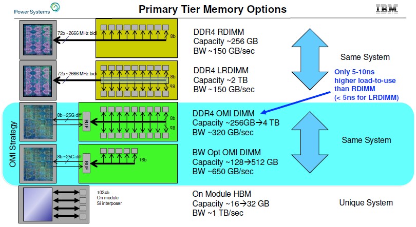
IBM’s OMI differential DDR memory, which uses a serial interface and a SerDes that is essentially the same as the “Bluelink” signaling used for NUMA, NVLink, and OpenCAPI ports on the processor, is very different from the normal parallel DDR4 interfaces, The specific DDR protocols, be it DDR4 or DDR5, sit out on the buffer chip on the memory card and the interface from the memory card to the CPU is a more generic OMI protocol.
This OMI memory under development back in 2019 delivered around 320 GB/sec per socket and from 256 GB to 4 TB of capacity per socket. And with a bandwidth-optimized version that cuts the memory module count by a factor of four and delivers somewhere between 128 GB and 512 GB of DDR4 capacity per socket, IBM could push the memory bandwidth on the Power9’ chip to 650 GB/sec and with the Power10 servers expected in 2021 it could push that up to 800 GB/sec using DDR5 memory that clocks a bit faster.
At the same time, for a Power9’ system expected to be delivered in 2020, IBM reckoned if it used HBM2 stacked memory, it could put 16 GB to 32 GB of capacity and deliver somewhere around 1 TB/sec of bandwidth per socket. That’s lots of memory bandwidth per socket, but it is not very much memory capacity.
For whatever reason – and we think whatever they were, they were not good ones, but it probably had something to do with Big Blue’s technical and legal difficulties with then-foundry partner Globalfoundries – the Power9’ system, very likely a four-socket machine with dual chip modules in each socket, never saw the light of day.
But the idea of a “bandwidth beast” was reprised as the Power E1050 as part of the Power10 midrange system lineup back in July 2022.
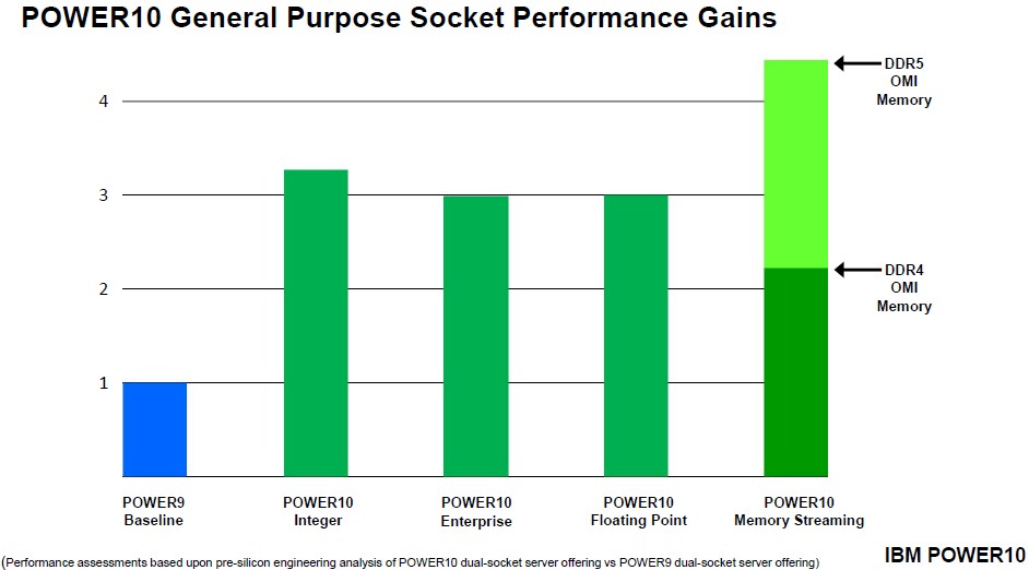
When the “Cirrus” Power10 processor specs were divulged in August 2020, IBM said that the chip had 256 GB/sec of peak memory bandwidth per core and 120 GB/sec of sustained memory bandwidth per core. There are 16 cores on the Power10 die, but to get better yields on the 7 nanometer process from Samsung, IBM’s new foundry partner, only a maximum of 15 cores are active. On the entry and midrange Power10 machines that came out last July, 4, 8, 10, and 12 cores are available in the SKU stack and the 15 core variant is only available in the high-end “Denali” Power E1080 system that scales to 16 sockets. It is not clear if those peak and sustained memory bandwidth figures were for DDR5 memory, but we suspect so. IBM did deliver the Power E1050 (and other Power10 machines) using OMI memory based on DDR4 memory, and said in its presentations that the memory streaming performance of the Power10 equipped with DDR5 memory would be 2X that of DDR4 memory.
The comparisons above are for single-chip Power10 modules. Double them up for dual chip modules, and then adjust for the downshifted clock speeds that are required to stay in the same thermal envelope as the single chip modules.
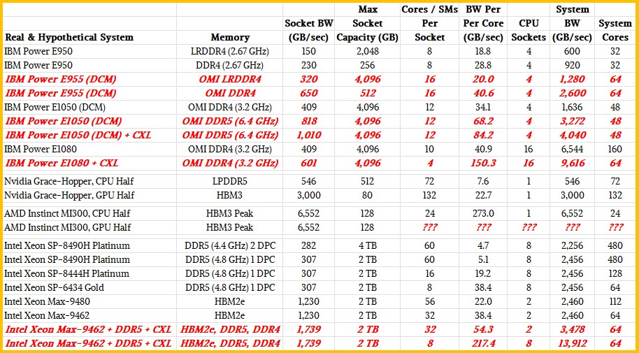
With the Power E1050 machine, the server has up to four Power10 DCMs and a total of 96 cores. Those eight chiplets had a total of eight OMI memory controllers and supported up to 64 differential DIMMs with DDR4 memory running at 3.2 GHz and delivered 1.6 TB/sec of aggregate bandwidth across the cores. That is 17 GB/sec of memory bandwidth per Power10 core at the peak of 96 cores in the system. But let’s do two things.
First, let’s cut the core counts way back. That fat configuration of the Power E1050 is using 12-core Power10 chips, but there is a 48-core variant that is using only six-core chips. (Yes, that is only a 37.5 percent yield on the Power10 cores.) That doubles the bandwidth per core up to 34 GB/sec. And if you shift to DDR5 memory running at 6.4 GHz, which is expensive and not really widely available at a sensible price, then you can get the memory bandwidth up to 68 GB/sec per core.
Now, in theory, if CXL memory extenders were available, you could push this real Power E1050 even further, You could burn 48 of the 56 lanes of PCI-Express 5.0 bandwidth per socket on CXL memory, adding six x8 CXL memory extenders at 32 GB/sec each yields another 192 GB/sec of memory bandwidth (with some addition latency on it, of course). That gets you to 1.8 TB/sec of aggregate bandwidth and 38 GB/sec of bandwidth per core. If IBM made the core counts smaller on each Power10 chiplet, then the memory bandwidth per core could be dialed up. At four cores per chip and 32 cores per system, you are up to 57.1 GB/sec of memory bandwidth per core. Moving to DDR5 memory plus CXL memory puts you at 84 GB/sec per core.
Enter The Hybrid Compute Engines
No one is saying this is cheap, mind you. But for certain workloads, it might be a better answer than porting code to a GPU or waiting for the hybrid CPU-GPU compute engines – Instinct MI300A from AMD, “Grace-Hopper” from Nvidia, “Falcon Shores” from Intel – come to market. And while these will have high memory bandwidth per core, the memory capacity will be constrained and therefore will be a lot more limited than what IBM can do with Power10 and Intel can do with the “Sapphire Rapids” Max Series CPU with hybrid HBM 2e/DDR5 memory.
The Nvidia Grace chip has 72 cores and sixteen banks of LPDDR5 memory with an aggregate of 512 GB of capacity and 546 GB/sec of memory per socket. That works out to 7.6 GB/sec of memory bandwidth per core. The Hopper GPU has 132 streaming multiprocessors – the analog to a core on a CPU – and a maximum of 3,000 GB/sec of bandwidth on its HBM3 stacked memory. (There are five stacks yielding 80 GB on the H100 accelerator.) That works out to 22.7 GB/sec of bandwidth per GPU “core” just to give you a frame of reference. If you treat all of the LPDDR5 memory on Grace as a kind of CXL-like memory, you boost the memory capacity of the CPU-GPU complex to a total of 592 GB and you boost the aggregate memory bandwidth to 3,536 GB/sec. Allocate the cores and SMs across that complex as you will. You can think of the GPU as a very expensive fast memory accelerator for the CPU cores and that works out to 49.3 GB/sec of memory bandwidth per Grace core or 26.9 GB/sec per Hopper SM.
The Power10 system as mentioned above is in this ballpark without much in the way of engineering.
With the AMD Instinct MI300A, we know it has 128 GB of HBM3 stacked memory across eight banks and across six GPUs and two 12-core Epyc 9004 CPU chiplets, but we don’t know the bandwidth and we do not know the number of SMs on the collection of six GPU chiplets on the MI300A package. We can make an educated guesses on the bandwidth. HBM3 is running signaling at 6.4 Gb/sec per pin and up to16 channels. Depending on the number of DRAM chips stacked up (from four to sixteen) and their capacities (from 4 GB to 64 GB per stack), you can get various capacities and bandwidths. Using 16 Gb DRAM, the initial HBM3 stacks are expected to deliver 819 GB/sec of bandwidth per stack. It looks like AMD might be using eight stacks of 16 Gb chips that are eight chips high per stack, which would give 128 GB of capacity and would yield 6,552 GB/sec of total bandwidth at the speeds expected when the HBM3 spec was announced last April. We think that the Epyc 9004 dies on the MI300A package have 16 cores, but only 12 of them are exposed to increase yields and probably clock speeds, and that would work out to an amazing 273 GB/sec per core of memory bandwidth across those Epyc cores as they reach into the HBM3 memory. It is hard to say how many SMs are on those six GPU chiplets, but it will probably be a very high bandwidth per SM compared to prior AMD and Nvidia GPU accelerators. But, again, 128 GB of total memory per compute engine is not a lot of capacity.
And, to curb our enthusiasm a bit, for thermal reasons, AMD might have to cut back on the DRAM stacks and/or the HBM3 memory speeds and therefore might not hit the bandwidth numbers we are projecting. Even at half the bandwidth per CPU core, this would be impressive. And again, for CPU-only applications, that GPU is a very expensive add-on.
Any CXL memory that might hang off this processor to add extra capacity would help on this front, but would not add very much to the bandwidth per core or SM.
We don’t know enough about future Intel Falcon Shores CPU-GPU hybrids to do any math at all.
HBM On The CPU And NUMA To The Rescue?
That brings us to Intel’s Sapphire Rapids with HBM2e memory, which also has a mode that supports both HBM2e and DDR5 memory at the same time. Sapphire Rapids is interesting to us not only because it supports HBM2e stacked memory in some variations, but because it also has eight-way NUMA scalability in other variations.
We think a case could be made to allow the creation of an eight-way, HBM-capable system that is goosed with both DDR5 and CXL main memory. Let’s go through it, starting with the regular Sapphire Rapids Xeon SP CPU.
As best we can figure, the eight DDR5 memory channels on the Sapphire Rapids Xeon SP can deliver just a tad bit more than 307 GB/sec of memory bandwidth on a socket. With one DIMM per channel running at 4.8 GHz, that is 2 TB of maximum capacity. With two DIMMs per channel, you can double the capacity per socket up to 4 TB, but you run at a slower 4.4 GHz and that yields only 282 GB/sec of memory bandwidth per socket. (This latter scenario is for a memory capacity beast, not a memory bandwidth beast.) With one DIMM per channel on that top-bin Xeon SP-8490H with 60 cores running at 1.9 GHz, that works out to a pretty skinny 5.1 GB/sec of bandwidth per core. If you drop down to the Xeon SP-8444H processor, which has only 16 cores – but they run at a higher 2.9 GHz so you get some of the performance back you lose by dropping cores – that works 19.2 GB/sec of bandwidth per core.
OK, if you wanted to push the memory bandwidth per core on a socket, you could switch to the Xeon SP-6434, which has eight cores running at 3.7 GHz. That would double the bandwidth per core to 38.4 GB/sec at the 4.8 GHz DDR5 speed. There is one fewer UltraPath Interconnect (UPI) link active on this processor, so the coupling on the two-socket server would be a little less efficient and would have a lower latency and lower bandwidth, too. That is in the same ballpark as a six-core Power10 chip using DDR4 memory running at 3.2 GHz and similar to what each core on the Grace Arm server CPU will see from its local LPDDR5 memory.
Now, let’s talk about the Sapphire Rapids HBM variant. The top bin Max Series CPU has 56 cores and the four HBM2e stacks have 64 GB of capacity and 1,230 GB/sec of aggregate bandwidth. That works out to 22 GB/sec of memory bandwidth per core. The low bin part has 32 cores across that same 1,230 GB/sec of memory, or 38 GB/sec per core. If you add the DDR5 memory on the socket, you can add another 307 GB/sec and if you add the CXL memory extenders, you get another 192 GB/sec. So now you are up to an aggregate of 1,729 GB/sec of memory across 32 cores, or 54 GB/sec.
Now, let’s push this to an extreme leveraging the NUMA interconnect to glue together eight Sapphire Rapids HBM sockets – which Intel is not allowing – and dropping the core counts to eight cores per socket running at 4 GHz. That yields 64 cores running at 4 GHz, or a little more oomph than a single Sapphire Rapids 60-core Xeon SP-8490H. But now, with HBM, DDR5, and CXL memory all added in, this eight socket box has an aggregate of 13,912 GB/sec of memory bandwidth, and a total of 217.4 GB/sec per core.
This would not be a cheap box, we are sure. But then again, neither is the Power E1050.
And if IBM dialed the cores down on the Power E1080 and added in CXL extenders, it could get something across 16 sockets that would be an aggregate of 6,544 GB/sec across the OMI memory attached to those 16 sockets plus another 3,072 GB/sec across six CXL memory modules on the PCI-Express 5.0 bus for a total of 9,616 GB/sec. How few cores do you want here? At four cores per Power10 SCM, that is 64 cores, which works out to 150 GB/sec of main memory bandwidth per core.
The point is, there is a way to build server nodes that focus on better memory bandwidth per core and thus are suitable for accelerating certain kinds of HPC and analytics workloads, and perhaps even a portion of AI training workloads. You will be more compute bound than memory capacity or memory bandwidth bound, and you have to be very careful not to have that terribly expensive memory not being taxed by not having enough cores pulling data out of it and pushing data into it.
By the way, we are less sure about how this bandwidth beast approach might accelerate AI training – perhaps only on pretrained models that are being pruned and tuned. We have a hunch that even GPUs have an imbalance between GPU core flops and attached HBM2e and HBM3 stacked memory bandwidth and that they do not run at anywhere near peak computational efficiency because of this.
We fully realize that none of this would be cheap. But neither are GPU accelerated machines. But having a better balance of compute, memory bandwidth, and memory capacity might be a better answer for certain workloads than chopping up memory into pieces and spreading datasets across dozens of CPUs. Admittedly, you really have to want to accelerate those workloads in a different way – and to program them across a memory hierarchy – to push the limits.
This is what thought experiments are for.


Many vendors have offered “high-bandwidth” server configuration options at many times during the last 20+ years. They have not sold well, typically because the cost savings of using a processor with fewer active cores is not large enough relative to the total system cost — customers realized that it was better to buy the extra cores of the more “mainstream” configurations even if those cores will only be useful for a portion of the workload.
More recently a new (and more technologically challenging) problem has dominated: cores don’t support enough memory concurrency to sustain higher bandwidth.
Little’s Law says that at a system latency load latency of 100 ns, a core that supports 20 outstanding cache misses (64B each) can sustain a read rate of 1280 Bytes / 100 ns = 12.8 GB/s.
For a “mainstream” DDR5/4800 server chip with 8 DDR5 channels (307.2 GB/s), it takes at least 24 cores to generate enough cache misses to fill the memory pipeline. This limitation applies (with different specific numbers) to any processor designed to work with a flat memory model and transparent caching.
GPUs get around the problem by having a whole lot more small cores.
The NEC Vector Engine processors take a different approach — memory concurrency is generated by vector operations that cover many cache lines. For long vector operations, a single core in an 8-core NEC VE20B processor can sustain 300-400 GB/s of the ~1500 GB/s peak bandwidth available from the 6 HBM modules. This requires that 30-40KiB of memory transactions be in flight at all times. With 64-Byte cache lines this would require more than 650 outstanding cache misses — not something that is easy to imagine from a traditional cache-based architecture.
I understand why we have GPUs. But not all code can be moved easily to GPUs and many datasets explode out beyond the very limited memory capacity of HBM. Hence my thought experiment. I see what you are saying, though, about the cache hierarchy. All I know is that by adding HBM, Intel is able to boost real-world HPC app performance on certain codes by 2X, which suggests to me that bandwidth is indeed a bottleneck. If I can get 2X or 4X or 8X by adding NUMA to Sapphire Rapids HBM, and not have to change codes and have a very large memory space, I think it might be a fair trade when fully burdened with the cost of altering applications added in.
The article and John’s comment are quite interesting (IMHO). Little’s Law may deal with how to keep the memory system busy, and one may also want to think about how to keep the cores busy. The number N of cores (or maybe threads) needed to keep memory busy when each core supports O outstanding cache misses, with cache-line size S, when the memory system has n channels, each of which has bandwidth B, and the access latency from DDR through the cache hierarchy is L (typ. 100ns) would be given by:
N = n B L / O S
The system may then have throughput, T, that matches the aggregate memory bandwidth: T = n B (if cores are fast enough). If each core runs at clock frequency C, and processes 64-bit data (8 bytes), then the number, P, of ops that the data processing algorithm should perform (for each input data) to keep all cores busy would be:
P = 8 N C / n B
and with N=24 cores running at C=2GHz with aggregate bandwidth nB=307GB/s, one gets a rather balanced P=1.25. But increase the number of cores, the clocks, or decrease memory bandwidth, and a more complex algorithm (higher P) is needed to keep cores busy. (Disclaimer: standard mis-interpretations and mis-calculations apply).
stacked memory bandwidth and that they do not run at anywhere near peak
Oh yeah! Feeding a 512-bit (64 bytes) vector engine (say AVX512) at 3.1GHz needs 200GB/s — super if the machine can provide it! With DDR5, if you can tame RAS-CAS-mataz latency with 2×8 consecutive BL16 burst reads (512 bytes from each of its 2 on-chip channels), so that cache line size is psychologically 1kB to Little’s Law (yet physically still 64B), then “Bang!” your core can ingest those 200GB/s provided by attached mems (with Lat.=100ns, and MSHR/LFB=20). The data has to be in 2 sets of sequential addresses though (should be ok for part of a matrix row, and column).
You can also see this graphically on tests of Xeons, EPYCs, and Ampere Altras (eg. Google: Andrei Frumusanu ice lake sp memory latency) where apparent latency from DDR through the cache hierarchy drops from 100ns for full-random reads, down to just 5ns for linear chain (sequential reads) (and then apply Little’s Law to the 64B cache line with that 5ns to get 200GB/s).