

Big Blue has become a big believer in using differential signaling to attach everything – and we mean everything – to the processor.
There is an upcoming kicker to the Power9 family, variously called the Power9’ (that is a prime symbol there, not an apostrophe) or the “Axone” chip or the Power9 AIO, short for Advanced I/O and distinct from the “Nimbus” Power9 SO (short for Scale Out) and “Cumulus” Power9 SU (short for Scale Up) processors. And with this Power9 kicker, IBM is going to be putting its ideas about using high speed SerDes circuits to link main memory to CPUs to the test. And, from the looks of things, this future Power9 chip and its Power10 follow-on will be getting an A+ in bandwidth.
IBM is, of course, no stranger to using buffered memory to boost the bandwidth of its processors and has been using them in its Power Systems line for as long as we can remember and, significantly, has been using its “Centaur” memory buffer with integrated L4 cache memory since the Power8 back in 2010 has been using memory buffers. Earlier this year we had a long chat with William Starke, the chief architect of the forthcoming Power10 processor, about memory bandwidth and the possibilities of using the “Bluelink” SerDes on the Power9 family of chips coupled with the OpenCAPI interface to create a low latency, high bandwidth interface to main memory, akin to the way IBM likes to link accelerators to the Power9 processing complex. (NVLink is just a protocol running atop the same 25 Gb/sec Bluelink signaling, providing coherency across the Power9 CPUs and Nvidia Tesla GPU accelerators.) In that conversation, we talked about how the OpenCAPI Memory Interface, or OMI, might work.
At the recent Hot Chips conference, Jeff Stuecheli, Power Systems architect at IBM, and Scott Willenborg, chief engineer for the Power9’ processor, revealed some of the feeds and speeds of the new OMI memory that will debut in the Power9’ chip early next year. As far as we know, this Power9 variant with high-speed memory was originally slated for delivery before the end of this year, so it looks like it has been pushed out. The delay in the Power9’ might have something to do with IBM and Nvidia not winning the “Frontier” exascale system deal at Oak Ridge National Laboratory or the “El Capitan” exascale system at Lawrence Livermore National Laboratory, since both organizations would have been pushing for prototypes based on the Power9’ just as they did with the Power8’ ahead of the Power9 systems used in their current “Summit” and “Sierra” systems, respectively. Or, just as likely, as Intel’s “Ice Lake” Xeon SP processors have also been moved further into 2020 as Intel has continued to have issues with ramping up its 10 nanometer chip manufacturing processes, IBM can take a small breather.
Call it Exxon’s Law: When one chip company takes its foot off the gas, the others tend to follow so they can work on getting better yields and doing more final tweaks on a future chip and then milking the existing chip for just a little while longer. . . . Anyway.
Stuecheli started out designing chips with the Power4 “GigaProcessor” as it was called, and this was IBM’s first undisputed champion RISC processor, coming in at 1.1 GHz back in 2001 and ramping up to 1.3 GHz with a crank on the clock and process tweaks a year later. IBM ramped up through the clock speeds with Power5, Power5+, Power6, and Power6+, kissing 3 GHz, and with Power7 and Power7+, it radically increased the cores (from two with the Power6 and Power6+ chips to eight with Power7 and Power7+) while pushing the clock speeds up to 5 GHz. Then the gigahertz ran out, as it always does with any chip design, and IBM had to go with more cores and slower clocks to deliver more throughput in the Power chips. So the Power8 and Power8’ chips topped out at 4 GHz with their 12 cores and the Power9 chips topped out at 4 GHz at 24 cores with four threads per core or 4 GHz at 12 cores with eight threads per core.
What has been clear to IBM for years, says Stuecheli, is that we need heterogeneous systems – what Stuecheli likes to call composable systems – because every machine needs to be accelerated in some fashion because a CPU cannot do everything as efficiently as is required due to the slowdown in Moore’s Law. We can’t know the ratio of CPU, GPU, and FPGA compute we might need ahead of time, any more than we can know how much memory capacity or memory bandwidth we might need, and that is why IBM has been adding more flexible interconnects, based on the 25 Gb/sec differential signaling, to its processors. At this point, the SerDes on the Power9’ chip will be down to two types: One for PCI-Express and one for Bluelinks that handle accelerators and main memory; the latter, says Stuecheli, is more power and area efficient than the PCI-Express 4.0 controllers can be because it operates in a very tight 25 Gb/sec signaling range. PCI-Express buses have to be able to slow down to offer backwards compatibility with prior devices, and that is a tougher problem that requires more transistors and more space on the die.
Take a look at the Power roadmap for the past decade to see how the memory and I/O has evolved:
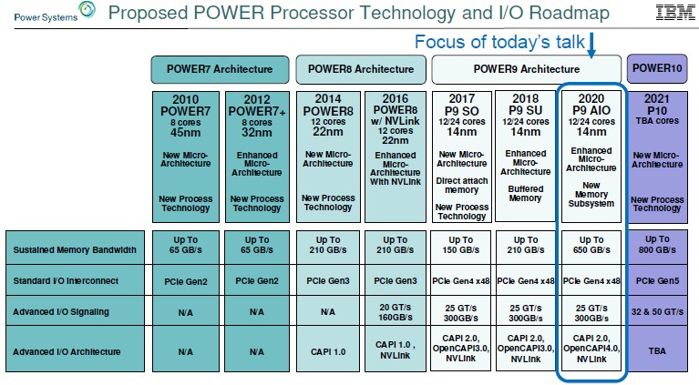
With the Power7 and Power7+ machines, IBM had an earlier generation of buffered memory that did not include L4 cache memory on the buffer chip, and the company could drive 65 GB/sec of sustained memory bandwidth per socket using wide banks of interleaved DDR2 main memory running at a relatively slow clock speed. X86 chips, by contrast, tend to not have buffers and therefore can’t hang as many memory sticks off a controller and therefore have to make it up with clock speed on the memory and memory controllers. And generally speaking, the X86 chips don’t make it up and usually have about half as much memory bandwidth per socket in a given generation as the then-current Power processor. With the Power8 chip in 2014, IBM cranked up the cores per socket by 1.5X but the memory bandwidth per socket by 3.2X with a shift to DDR3 and then DDR4 main memory, yielding a peak sustained bandwidth of up to 210 GB/sec per socket thanks in large part to the Centaur memory buffer and L4 cache controller. With the Power8’ chip in 2016, the memory subsystem stayed the same, but IBM added native Bluelink signaling running at 20 Gb/sec and delivered a total of 160 GB/sec bi-directionally (meaning 320 GB/sec in total) across the aggregated Bluelink lanes.
With the jump to the Power9 chips, IBM bifurcated its chips. The Nimbus Power9 chips were aimed at less expensive scale-out machines where core counts were more important than memory bandwidth, so IBM added DDR4 controllers directly onto the chip and did away with the Centaur buffer. If could use faster memory, like X86 servers, but it could only hang half as many memory sticks off the eight controllers on the die, and therefore memory bandwidth per socket actually dropped by 28.6 percent to 150 GB/sec. IBM doubled up PCI-Express capacity by supporting the 4.0 protocol with its on-die peripheral controllers, hitting 96 GB/sec bi-directionally (192 GB/sec duplex), and it boosted the Bluelink SerDes by 25 percent to 25 Gb/sec signaling and added more lanes to get up to 300 GB/sec bi-directionally (600 GB/sec total) across the Bluelinks (with a total of 96 lanes). Some of this bandwidth was carved up for the NVLink 2.0 protocol and some for OpenCAPI devices. The CAPI 2.0 interface ran over PCI-Express 4.0 and saw a 4X performance increase relative to the CAPI 1.0 protocol that ran on the PCI-Express 3.0 protocol supported on the Power8 and Power8’ chips. IBM also put 16 Gb/sec NUMA links on the die to interconnect two processors or four processors, and some of the faster Bluelink ports were used to scale systems to eight, twelve, or sixteen sockets.
A picture might help here, so here is how the Nimbus, Cumulus, and Axone Power9 chips differ from each other in terms of I/O and memory connectivity:
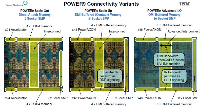
You can see that the eight DDR4 memory controllers – four on the top right and four on the bottom right – with the Nimbus Power9 scale out processors take up quite a bit of space. This is no more than any other architecture, but clearly staying with Direct Memory Interface (DMI) memory controllers and putting a lot of the memory controller circuits out onto the buffer chip is a way to save transistor budget and area on the CPU die. It looks like about a 30 percent savings to our eye just across the memory controller circuits.
With the Cumulus Power9 chips, memory bandwidth, memory capacity, and lots of threads were the key for IBM’s enterprise-class machines, and so these scale up processors kept the Centaur buffers and their L4 cache memory. By shifting staying with the DMI memory controllers used in the Power8 and Power8’ chips, IBM had the ability to add up to 96 PowerAXON ports – that’s the new name for the Bluelink ports – to the chip. Significantly, the DMI controllers used in the Cumulus Power9 chips offered 3X the bandwidth per chip area as the DDR4 controllers used in the Nimbus Power9 chips. The Cumulus chip had three local NUMA ports running at 16 Gb/sec compared to two for the Nimbus Power9 chip. (IBM calls these SMP ports, but they are really NUMA ports.)
With the Power9’ or Power AIO chip coming out in 2020, IBM is changing the memory controllers to make use of the same Bluelink SerDes used to link accelerators to the Power9 processing complex to drive a different memory buffer chip that does not have L4 cache on it. This OpenCAPI Memory Interface has 6X the bandwidth per chip area as the on-chip DDR4 memory controllers used in the Nimbus Power9 chips. Instead of keeping the memory controller count at eight and using the gain in bandwidth to reduce the memory controller area on the Power9 chip, IBM is going to double up the controllers with the OMI approach to sixteen. This will allow IBM to double up the bandwidth while at the same time allowing it to have a high number of memory slots per socket that can in turn use less capacious memory sticks that also cost less per unit of capacity.
Well, not precisely. If you drill down into what IBM divulged at Hot Chips, it will actually have two different variations of the OMI memory stack with the Power9’ chip. In one variant, there are relatively high capacity DDR4 memory sticks that in a fully populated system deliver between 256 GB and 4 TB per socket and around 320 GB/sec of sustained memory bandwidth. But there is another variant that has fewer memory chips on the DIMM, meaning not only is there less capacity per memory stick but also more memory bandwidth available per DIMM. This variant can deliver 650 GB/sec of sustained memory bandwidth and from 128 GB to 512 GB per socket of memory capacity.
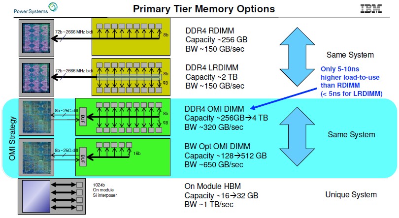
As you can see, and as Starke hinted to The Next Platform earlier this year, with OMI memory IBM can get two thirds of the way to the bandwidth of HBM2 memory used on GPUs and a few upcoming CPUs without having to resort to memory stacking on an interposer. And the capacity is anywhere from 4X to 32X higher.
This is really significant. IBM has effectively created DDR5 industry-standard buffered memory years before it will be on the market, and this memory will be absolutely competitive with HBM stacked memory, which is a pain in the neck to deal with.
IBM is partnering with Microchip to use its serial Smart Memory Controller 1000 chip, which implements eight lanes running at 25 Gb/sec, in the initial OMI memory used in the Power9’ systems. With the Centaur buffer chips, an additional 10 nanoseconds or so of latency was added by the buffer compared to using the raw DDR4 controller. This wasn’t a painful latency add for memory reads and writes, and the L4 cache masked a lot of it. With OMI memory and the evolving JEDEC DDR5 spec that the Power10 chip will support, the buffer chip has fewer ports and no L4 cache, so the latency add has to come down. And according to Willenborg, the overhead on registered DDR4 DIMMs is between 5 nanoseconds and 10 nanoseconds, and on load reduced DIMMs, it is around 4 nanoseconds.
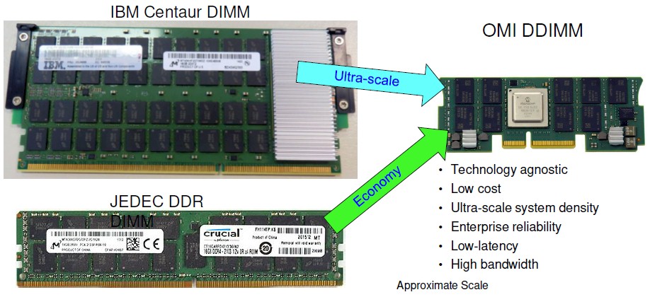
“I will be surprised if other memory buffer solutions achieve the latencies we have done with this,” says Willenborg. There are a number in the works, apparently. The SMC-1000 is just a write buffer, and it does not offer caching and it implements one memory channel of eight lanes running at 25 Gb/sec; there are a total of sixteen slots per socket. The Centaur chip had 16 MB of L4 read cache and implemented four memory ports, allowing for sixteen slots per socket because you could hang two channels off a single controller.
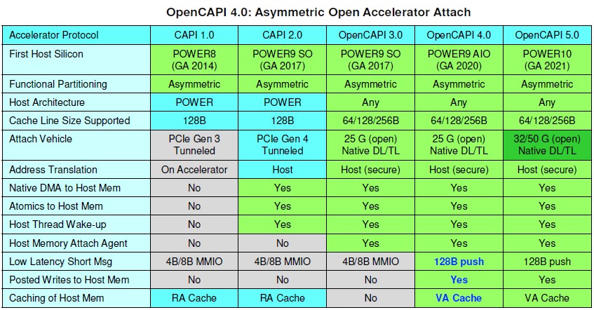
With Power10 in 2021, IBM is boosting the Bluelink ports to 32 Gb/sec and 50 Gb/sec speeds, as you can see from the roadmap, and it looks like the OMI memory could be using the 32 Gb/sec ports and boost the aggregate memory bandwidth per socket to 800 GB/sec. That’s even closer to what a GPU can do with HBM2 stacked memory these days. And if IBM pushed up to 50 Gb/sec signaling – and it is a wonder as to why it will not do this – then it could probably hit 1.2 Tb/sec. That, by the way, was the target bandwidth of the “Volta” Tesla GPU accelerator, which Nvidia did not hit with HBM2.
It makes you think about how the balance of power could change in compute. Pendulums do tend to swing back and forth, and maybe some work will swing back to the CPUs if they have enough of the right instructions and enough parallelism.

For IBM, AI Inference Is The Most Important HPC
All of the commercial platform creators in the world, since the dawn of time, which arguably started in the enterprise in April 1964 with the advent of the System/360 mainframe, wants the same things. They want to create a flexible, integrated, and useful system where data can be stored and …

Kubernetes Clusters Have Massive Overprovisioning Of Compute And Memory
In the ten years since Google released Kubernetes to the open source community, it has become the dominant platform for orchestrating and managing software containers and microservices, along the way muscling out competitors like Docker Swarm and Mesosphere. (Remember those? In a decade, you won’t.) Those building software stacked embraced …

Injecting Machine Learning And Bayesian Optimization Into HPC
No matter what kind of traditional HPC simulation and modeling system you have, no matter what kind of fancy new machine learning AI system you have, IBM has an appliance that it wants to sell you to help make these systems work better – and work better together if you …
Wow wow wow! Power9 and Power10 will beat the market! This is great!
IBM always ahead… let’s see if the market buys this. I foresee a cloud full of POWER10s with GPUs/Accelerators attached with that bandwith highway compared to existing x86 based solutions