

Imagine, if you will, that Nvidia had launched its forthcoming “Grace” Arm server CPU three years ago instead of early next year. How much better would Nvidia be fairing in the gaming and cryptocurrency downdraft that is impacting its sales today?
Sometimes, little changes make a big difference in the CPU market.
For instance, we have talked about how fortunate AMD has been that it switched from using its own foundry spinout, GlobalFoundries, as its sole supplier of CPU wafers and to using Taiwan Semiconductor Manufacturing Co to make the core complexes for its Epyc server chips.
That decision, as much as any architectural one, has been central to the success that AMD has had, especially in light of GlobalFoundries’ failure to bring 10 nanometer and then 7 nanometer processes to market, which had a huge and arguably detrimental impact on IBM’s Power9 and Power10 processors. Enough for IBM to sue GlobalFoundries last year just months before that chip manufacturing company (which is the combination of AMD, IBM, and Chartered Semiconductor fabs) decided to go public to raise some money to fuel its growth.
Nvidia clearly had aspirations of its in server CPUs before the AI wave swamped the hyperscaler and cloud builders and splashed into enterprise datacenters, lifting Nvidia’s datacenter business from an interesting aside to its largest and most profitable division.
In January 2011, as Nvidia was only then accelerating HPC simulation and modeling workloads with GPUs and the machine learning revolution was just getting going in academic centers, Nvidia launched its “Project Denver” Arm server CPU initiative. Three years later, the word on the street was that Nvidia had come up with its own CPU instruction set architecture (ISA) and was emulating the Arm ISA and the Intel X86 ISA on top of that. Then there was a lawsuit between Nvidia and Intel over intellectual property, and apparently, if the rumors are right, Nvidia agreed it would never do X86 emulation on a CPU. And then it canned the whole server CPU effort.
It wasn’t until Nvidia recaught the vertical integration bug again a few years ago, as it bought Mellanox Technology, that it reconsidered going back into Arm CPUs for servers. But imagine if Nvidia had launched a 10 nanometer part four years ago, ahead of AMD’s “Rome” Epyc 7002s and Intel’s “Ice Lake” Xeon SPs – and a 10 nanometer Grace that had some of the memory coherency features that ended up in IBM’s Power9 processors so the “Volta” GV100 and “Ampere” GA100 GPUs could mindmeld with CPUs over NVLink. That sure would have been fun. . . .
Suffice it to say, had that happened, Nvidia would have been well positioned to capture a significant slice of the CPU market against a weakening Intel and a not-yet strong AMD. As many of you have heard us say before, to quote a very wise financial planner, chief financial officer, and university professor we once knew: “The best time to do anything was ten years ago. The second best time is right now.”
It with that alternate history in a thought experiment and that spirit in mid that we consider the revelations about the Grace CPU that Nvidia made recently at the Hot Chips 34 conference. There wasn’t much, but we know a little more and also have some insight into Nvidia’s thinking about the Grace design thanks to the talk given by Jonathan Evans, an Nvidia distinguished engineer and the architecture lead for the Grace chip.
We now know officially – as we originally expected – that Grace will have cores that hew to the Armv9 specification unveiled in March 2021.
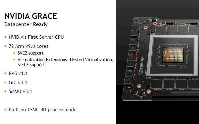
Grace cores will also sport vector math units that adhere to the SVE2 second generation vector math standard that Arm and Fujitsu cooked up for the HPC space and that has been extended to the mixed precision and matrix math of the machine learning era. Evans did not specify the width of these vectors, but we expect that a pair of 128-bit SVE2 vectors in the current “Perseus” Neoverse N2 cores from Arm Holdings will not do the trick, and by definition we know that the pair of 256-bit SVE vectors used in the “Zeus” V1 cores from Arm Holdings are not in Grace either because they are not SVE2 vectors. We think it is highly likely that Nvidia has licensed material from Arm Holding’s future “Poseidon” Neoverse N3 and V2 cores (that is our name for those future cores) to create the Grace cores and their vectors, and we think the Grace cores could have a pair of 128-bit or a pair of 256-bit vectors, but probably not a pair of 512-bit vectors. Intel has not been precisely successful with a pair of 512-bit AVX-512 vectors in the Xeon SP design. We did some estimating back in March and figured Grace would run at between 2 GHz and 2.3 GHz and with a pair of 256-bit vectors would do maybe 2.3 teraflops to 2.65 teraflops peak with 72 active cores.
Evans made a big deal out of the fact that Grace supports all of the Arm server standards, and rightfully so, which include:
- Arm Server Base System Architecture (SBSA)
- Arm Server Base Boot Requirements (SBBR)
- Arm Memory Partitioning and Monitoring (MPAM), and
- Arm Performance Monitoring Units (PMUs)
By doing so, Nvidia is assured that operating system and application software already written for other Arm chips will run on Grace. There is no talk of an X86 ISA overlay on the Grace processor, and given the history, we don’t expect one unless Pat Gelsinger, Intel’s chief executive officer, is a lot harder up for money than we already believe is the case. (If would be a lot of fun for that X86 emulation mode to be revived in some way on Grace, or maybe in a future Nvidia Arm server chip.)
Nvidia keeps saying that Grace is a 72 core processor, but if you look at the die shot, you can see that there are actually 84 cores on the die. You can also see that the layout could easily accommodate 96 cores with the addition of one more row of cores – which would actually be balanced and which leads us to believe Nvidia was trying to get to 96 cores with Grace and had to back it off a bit to keep the Grace superchip double whammy and its LPDDR5 memory all under 500 watts. Getting to 96 cores might take a 3N process from TSMC to accomplish within this power envelope and within the clock speeds that Nvidia is aiming for, and that might be a Grace 2 chip for 2024.
Those extra 12 cores on the Grace die that Nvidia is not talking about are just there to improve yield, just like the full number of streaming multiprocessors (SMs) is never initially available on an Nvidia GPU. Sometimes, the extra cores or SMs are never, ever available. Yields never get to 100 percent. (But if you really wanted a higher core count, you can probably ask Nvidia to do a deeper bin sort.)
The Grace CPU is built on the same custom 4N process from TSMC that the “Hopper” GH100 GPU that is coming soon – very likely at the fall GTC conference in September – uses for its manufacture. The 4N process is a refined 5 nanometer process with additional tweaks for transistor shrinkage and added switching performance.
One other thing we learned about Grace is that it will always be part of a superchip dual-chip complex. Either Grace-Grace or Grace-Hopper – never just one Grace by itself. The NVLink 4 ports coming off the Grace chip have 900 GB/sec of aggregate bandwidth, and the new bit of data is that this interface can move data at 1.3 picojoules per bit, which Evans said was 5X as energy efficient as a PCI-Express interconnect and offering 7X the bandwidth of PCI-Express 5.0 x16 links.
That fat pipe between Grace and Hopper means that the CPU and the GPU can use the other’s memory almost directly. So in a sense, the 80 GB of HBM3 memory on Hopper is a high bandwidth memory for the CPU and the 512 GB of LPDDR5 memory on Grace is a fat auxiliary memory for the GPU. They have a shared virtual address space across those memories, and the GPU has access to pageable memory, memory page tables are shared across the devices, and the malloc and memap pointers used in CPU architectures can be used to access the GPU memory. Which leads us to wonder if Nvidia will eventually offer a coreless Grace CPU as a special memory extender for those who just want to run fatter memories on their Hopper GPUs.
Evans also talked a bit about the scalable coherency fabric, or SCF, at the heart of the Grace chip. Take a look:
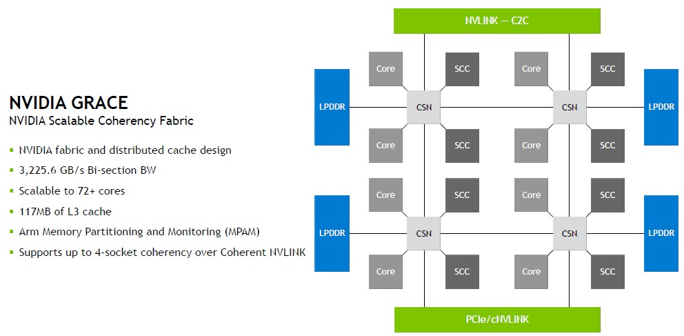
This obviously does not show all of the cores in the Grace die, but just illustrates the nature of the fabric linking the cores, their main memory controllers, their scalable coherent caches (SCCs), and their interconnects. In the version of Grace coming to market, there are 177 MB of total L3 cache across those SCCs.
“The CPU cores and the SCF cache partitions, also known as SCCs, are distributed throughout the mesh,” Evans explained. “The cache switch nodes, or CSNs, write data through the fabric and act as the interface between the cores, caches, and the rest of the chip and enable the incredibly high bandwidth throughput you see in Grace. The Grace-Hopper superchip also supports multi-socket coherency and up to four chips may be used to create a four superchip coherent node.”
That sounds cool. The Grace SCF is not based on any Arm Holdings on-chip mesh or ring interconnect, which is immediately obvious given its topology. But Evans confirmed that this is the case.
Here is what the block diagram of Grace looks like:
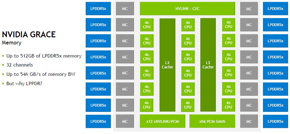
The Grace chip has 16 memory controllers and 16 banks of low-power LPDDR5 main memory – the kind you use in laptops and other embedded devices. There is one 900 GB/sec chip-to-chip (C2C) link and what looks like two PCI-Express 5.0 controllers. One that has 56 lanes running plain vanilla PCI-Express 5.0 and one that has twelve lanes of NVLink (cNVLink in the diagram above) that also seems to speak PCI-Express protocols. The latter is used to hook Grace-Grace superchips to Hopper GPUs and other devices.
So why LPDDR5 memory, you ask. Well, Evans explained that in this table:
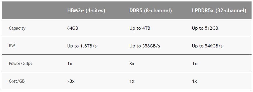
With 32 memory channels and one chunk of memory per channel, Nvidia can drive 546 GB/sec out of 512 GB of main memory and still be in the same cost profile of much fatter – but much slower – plain vanilla DDR5 main memory. Nvidia is eliminating any choices about memory capacity or bandwidth by hard-wiring the LPDDR5 memory, which may irk some customers. But there is method in Nvidia’s madness here.
Evans gave a great example of this. Say, for example, you wanted to do some training and inference on the GPT-3 model for natural language processing, which has 175 billion parameters. If you want to be very efficient, you would have data and processing in 8-bit, quarter-precision FP8 floating point mode.
To do inference from the model all in memory, you need a total of 175 GB of capacity, and that won’t fit into Hopper’s 80 GB of memory. But it certainly fits into the 512 GB of Grace memory, and spread across their combined memories, there is 417 GB left over on Grace.
To do training, you need a much more massive 2.5 TB of memory to run GPT-3. If you were just using HBM3 memory on the Hopper GPUs, you would need 32 GPUs to fit the GPT-3 training set into memory. But if you use Grace-Hopper superchips, you only need four units to reach 2.3 TB and five puts you over the top. The chart from Evans suggested that eight Grace-Hopper superchips was the right answer, probably to have some memory left over in the Grace hosts so they can do some management work and run a Linux operating system.
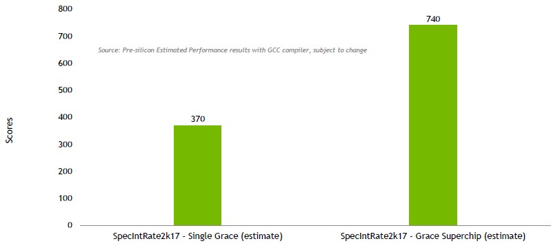
For the record, here is the estimated SPEC integer performance for Grace:
And here are the estimates for memory bandwidth performance on a single Grace chip using parts of the STREAM benchmark. On Hopper-to-Grace memory performance, Nvidia has a homegrown test showing reads at 429 GB/sec, writes at 407 GB/sec, and a combination of reads and writes at 506 GB/sec. Clearly, we can see where Nvidia is optimizing the coherent memory performance – across a mix of read and write operations across a mix of local HBM3 and CPU LPDDR5 memory. Getting somewhere around 92.7 percent of peak theoretical bandwidth across that CPU memory is pretty good, and while it is not anywhere near as fast as the 3 TB/sec across the HBM3, there is no way to have both fat and fast memory across one memory subsystem that is also manufacturable and affordable. This splits the difference nicely.
By the way, these are simulated results, not actual tests on early silicon. It is not clear when Nvidia is expecting to get silicon back from TSMC.


The Performance Of MLPerf As A Ubiquitous Benchmark Is Lacking
Industry benchmarks are important because, no matter that comparisons are odious, IT organizations nonetheless have to make them to plot out the architectures of their future systems. The MLPerf suite of AI benchmarks created by Google, Baidu, Harvard University, Stanford University, and the University of California at Berkeley had a …

Los Alamos Pushes The Memory Wall With “Venado” Supercomputer
Today is the ribbon-cutting ceremony for the “Venado” supercomputer, which was hinted at back in April 2021 when Nvidia announced its plans for its first datacenter-class Arm server CPU and which was talked about in some detail – but not really enough to suit our taste for speeds and feeds …
Arm Neoverse Roadmap Brings CPU Designs, But No Big Fat GPU
Spoiler alert! A lot of neat things have just been added to the Arm Neoverse datacenter compute roadmap, but one of them is not a datacenter-class, discrete GPU accelerator. And another one that is also not there is a more specific matrix math accelerator like the ones that Intel (well …
Has NVIDIA said whether Grace-Hopper (or Grace-Grace, for that matter) will be a mainboard chip, or will come on an add-in board just like its GPUs?
It has not. But if you look here:
https://www.nextplatform.com/2022/03/25/nvidias-grace-arm-server-chip-is-a-game-changer/
at the system designs, you will see a system board with one Grace and two Hoppers and two CX7s. It looks sorta MiniITX-ish. But ecven still, it looks like it will be an SXM PCB of some sort.
Jonathan Grace? Would that be Jonathan Evans, by any chance?
Ya know, I saw that and I thought I fixed it. Every time the phone rings, my L1 buffer flushes and my L2 pointers ain’t great. The phone rings a lot.