

We are still chewing through some of the announcements that came out of Intel Investor Day and the ISSCC 2022 chip conference, and one of the things we want to circle back on is the “Falcon Shores” hybrid CPU-GPU that Intel is working on for future servers.
Given all of the work the industry has done to more tightly couple CPUs and GPUs, not the least of which being getting the PCI-Express bandwidth train back on the tracks and running on time with a two-year cadence of bandwidth doubling and getting the industry to rally around the CXL protocol put forth by Intel, it may seem odd that Intel is talking, once again, about making a frankensocket that crams two distinct types of compute into a single socket.
But here we go again, and Intel is, of course, not the only one. In one respect, then, certain kinds of servers are going to be glorified laptops, many of which have used a hybrid CPU-GPU – what is sometimes called an XPU, where the X is a variable and denotes multiple kinds of compute – for years and years now. For certain kinds of workloads, such XPUs are fine so long as the balance of compute is right and the cost of integrating the components is not exorbitant.
The future Intel CPU-GPU XPU is code-named “Falcon Shores” and will very likely carry the Xeon brand since it is going to fit into a Xeon socket. The Falcon Shores XPU was not discussed by Intel during its Investor Day keynote, when the Xeon roadmap was updated, and when we talked privately about that roadmap with Intel’s techies they didn’t bring it up, either, because they were saving that revelation for Raja Koduri, who is general manager of the new Accelerated Computing Systems and Graphics business, abbreviated AXG by Intel.
Koduri did not say much about Falcon Shores, but given that it will be based on “angstrom era” process technologies, then we should not expect this XPU until sometime in the first half of 2024 using the 20A processes from Intel Foundry Services.
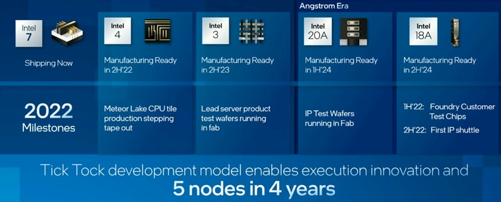
The 20A process is based on Intel’s first implementation of the RibbonFET, gate-all-around arrangement of transistors, and when Intel talked about the process roadmap last year, it was expected to come to market sometime in the first half of 2024, and that 20A process is still on track as far as we know. (Given recent history with Intel on 10 nanometer and 7 nanometer processes, you have to check – and check often.) Based on the current roadmap above, it looks like the 18A process has been pulled in, from expected first use in 2025 to the second half of 2024. The 18A process will have an improved RibbonFET transistor design and process refinements. The 20A process is significant because it is here where Intel expects to reach performance per watt leadership with the 3 nanometer technologies that Taiwan Semiconductor Manufacturing Co expects to have in the field at the same time.
Intel could, of course, in theory build a frankensocket right now based on a cutdown “Sapphire Rapids” Xeon SP and a cutdown “Ponte Vecchio” Xe HPC GPU accelerator. But such a chip complex would require a substantial reworking of the CPU and GPU halves and therefore a pretty sizable engineering budget for perhaps no gain. And it would almost certainly require a custom Xeon socket because this beast would be quite large indeed. And this engineering money for a Sapphire Rapids-Ponte Vecchio XPU would be spent during a time when Intel has been having trouble delivering the discrete (meaning not co-packaged or co-died) Sapphire Rapids CPUs and Ponte Vecchio GPUs for the 2 exaflops “Aurora” supercomputer that has had many incarnations and that Argonne National Laboratory has been waiting to see for nearly four years.
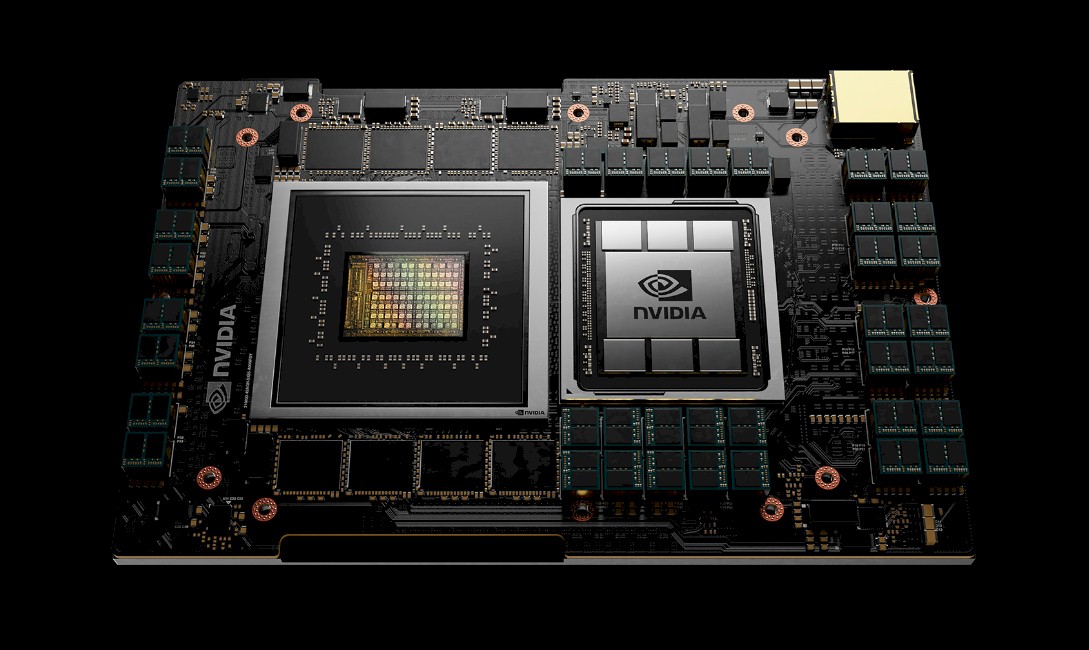
If Intel had aspirations to beat Nvidia with its “Grace” Arm CPU and its “Hopper” GPU compute complex, to the server XPU punch, that is not going to happen. But Intel will be a fast follower if this idea takes off – and we think in many cases it will take off despite the fact that the ratios of CPU and GPU compute are relatively fixed. Nvidia is creating a single module with a Grace CPU socket with DDR5 memory and a Hopper GPU socket with HBM2e memory, all of the compute cross-coupled with fat NVLink 4.0 pipes in a shared memory complex.
The Falcon Shores chip will literally plug into a Xeon SP socket and will not require any changes to the server complex in terms of power or thermals – other than a BIOS update, we presume. Given the timing and the recent Intel Xeon SP roadmap, that means the Falcon Shores chip will plug into the same sockets as the future “Granite Rapids” Xeon SPs expected in 2024, based on the more detailed roadmap we cobbled together based on hearsay and rumor and speculation, the Falcon Shores XPU will be a member of the “Mountain Stream” platform and will not plug into the “Eagle Stream” platform used by Sapphire Rapids Xeon SPs and their kicker “Emerald Rapids” Xeon SPs. This matters because customers who buy Eagle Stream platforms this year and next will not be able to use the same server types (or servers they already have in the field) to add hybrid Xeon-Xe XPUs.
That Xeon SP angle is important when talking about the HPC market for sure, and probably for the AI inference market, too.
“More than 85 percent of the world’s supercomputers are based on Xeon processors,” Koduri explained in his presentation. “Billions of lines of code are optimized for it, including the world’s most important HPC and AI applications. This platform offers us an incredible starting point to launch from. Our strategy is to build on this foundation and extend this to even higher compute and memory bandwidth.”
To be fair, there are a number of very large supercomputers that are based on a combination of Intel CPUs and Nvidia GPUs, and a fair number are soon going to be based on the combination of AMD CPUs and either Nvidia GPUs or AMD GPUs. But the point is well taken that a lot of HPC work is still done on CPU-only machines because the task of supporting GPU accelerators is still hard. Still, how many Intel CPUs were not sold because a GPU accelerator was sold in its place? The number is now easily millions, although you could argue that for capability class machines, had it not been for the advent of GPU compute, no one would have built pre-exascale, much less exascale, systems.
But here is another data point as you consider Falcon Shores. A decade or so ago, when machine learning was still being commercialized by the cloud builders and hyperscalers, mostly for their own use, Intel was fond of bragging that 95 percent of the world’s datacenter inference was done on Intel’s Xeons. Now, that percentage is down to 75 percent, according to statements made recently by the chip designer and maker. (Intel is the last one to do both and deserves acknowledgment for that.) Let’s say for the sake of argument that all of the inference done in the datacenter has quadrupled in the past decade; that’s a compound annual growth rate of 41.4 percent. That would mean, if you do the math, that Intel has grown its inference share by 3.2X, which sounds like a lot. But all of the others hawking inference wares now have a quarter of the market and have grown at 20X. So we think that having an integrated GPU means being able to do more complex inference than is possible with the AMX matrix math units and with absolutely lower latency than is possible with a discrete Xe HPC GPU.
The amount of inference out there could go up by another factor of 4X – or more – in the coming decade, so there is a lot of matrix math at stake here. It makes the aggregate amount of 64-bit and even 32-bit HPC simulation and modeling look miniscule. Our best guess is Intel will drop to 40 percent of the base (but still double its share of inference compute on its Xeon CPUs) unless conditions change.
Falcon Shores is as much about changing the conditions as Nvidia’s Grace/Hopper is. And all within the confines of plain old Mountain Stream server socket.
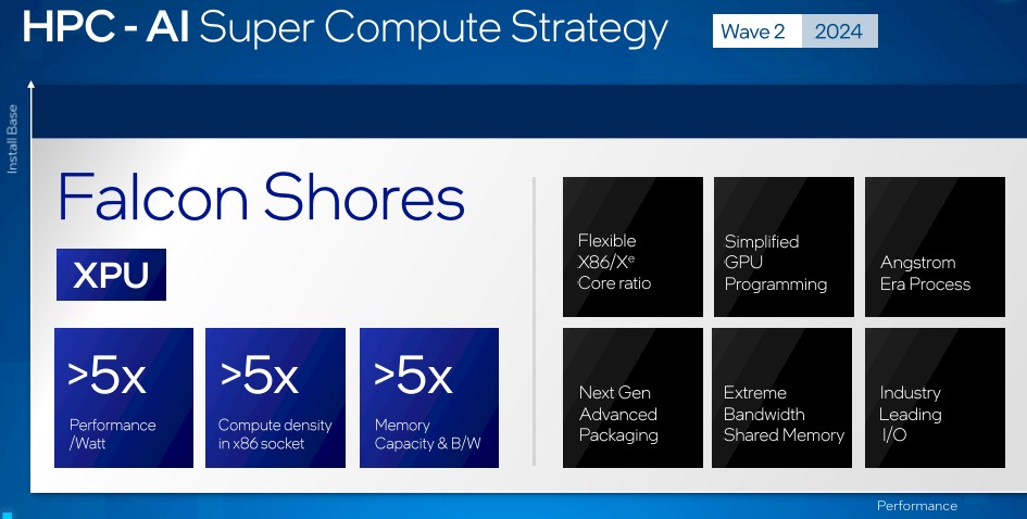
“We expect Falcon Shores to deliver more than 5X performance per watt, more than 5X compute density, and more than 5X memory capacity and bandwidth improvement – all in a single socket with a vastly simplified GPU programming model,” Koduri said, laying down the gauntlet.
Presumably those performance increases are compared to an “Ice Lake” Xeon SP processor. The chart says it is compared to “current platforms in February 2022,” so we assume that is what Intel means.
That last declaration about the “vastly simplified” GPU programing model is intriguing. It got us to thinking. What if Intel made a kind of emulator for the GPU so it could look like an AVX-512 vector engine or an AMX matrix engine and use the same instructions? What if the CPU thought the GPU was native? There could be a native oneAPI offload across what we presume will be UltraPath Interconnect links between the CPU and GPU parts of the chips, although they could be Xe links. That would be neat, wouldn’t it?
Koduri added that the Falcon Shores XPU would have what he called “extreme bandwidth shared memory,” which we think could mean a mix of support for DDR and HBM memories, and with a large pool of cheap and fat DDR complementing the fast and skinny HBM. But this could be something else entirely.
Hmmmm. . . .
As you can see from the chart above, Intel is promising a flexible ratio of X86 and Xe cores across the Falcon Shores device. This is probably more a statement about how Intel intends to use the yield curve for the 20A process. At the front end, there will be plenty of partial duds, and the mix of CPU and GPU cores might be more of a reflection of low process yield than a desire to have a complicated SKU stack. The point is, why throw away any parts? A Xeon SP chiplet that doesn’t make the cut in actual Granite Rapids – or said more precisely there are too many of them with low core counts so supply exceeds demand – and a Ponte Vecchio successor (we don’t have a code name yet) chiplet that doesn’t make the cut for the same reason can both find homes in a Xeon socket as part of an XPU.
The real worry is what is the incremental cost of adding the GPU to the CPU complex, and what will Intel charge to customers who want to buy it. The cheapest flops in the datacenter, as we have demonstrated time and again, are the integrated graphics engines that are available on Xeon E3 chips that are really Core i5/i7 workstation processors put into a Xeon socket. We are also a little bit worried about having CPU and GPU capacities locked own inside of a socket, but in some cases, this might not be much of a concern if Intel gets the ratios right. We strongly suspect that Intel will not allow the mixing of Xeon SP CPUs and Xeon-Xe XPUs within the same system, but there would, of course, be a way to add supplementary GPU capacity over PCI-Express/CXL links within a chassis.
“We are super-excited about this architecture as it brings acceleration to a much broader range of workloads than the discrete solutions,” Koduri claimed.
We get the simplicity of just using a Xeon socket, and think that some sort of emulation shim is part of the picture, but that is just a hunch. (And if not, why not add it now?) We look forward to seeing the architecture of this Falcon Shores hybrid and watching if customers go for it. Nvidia will be going first with its Grace/Hopper complex as well as, we presume, discrete and beefier Grace CPUs and Hopper GPUs that create a DGX/HGX complex like the AMD Epyc 7003 and Ampere A100 GPUs do in the DGX-2 today.


Hope it isn’t going to consume Aurora (wall) power as well, including cooling power
HA! Yes, Indeed. I also presume not!
“There could be an native oneAPI offload across what we presume will be UltraPath Interconnect links between the CPU and GPU parts of the chips, although they could be Xe links.”
I thought a primary feature of cxl is to provide the biased cache coherency, which effectively pools up all the cache coherency transfers while the slave has ownership. Why would they abandon that and return to UPI? Wouldn’t that also require the GPU to have the complicated and proprietary home agent?
Well, there are three different ways to skin that potential cat, and I just suggested one of them. I guess we will see.
“Koduri added that the Falcon Shores XPU would have what he called “extreme bandwidth shared memory,” ”
Why wouldn’t this just be another implementation of the Rambo L2 SRAM ache used on Ponte Vecchio?
One of the recent Intel patent applications shows an entire base layer with embedded sram chiplets. See Fig 32 of US20210150663.
I suppose it could be. But I was thinking higher up in the memory hierarchy. We are always limited by our initial assumptions.