

No question about it. Intel had to get a lot of moving pieces all meshing well to deliver the “Ice Lake” Xeon SP server processors, which came out earlier this month and which have actually been shipping to a few dozen select customers since the end of 2020.
Getting the 10 nanometer manufacturing processes finally working was key, of course, because it is the change in transistor sizes that allows for the increase in the core count that drives per-socket throughput and also allows for clock speeds to be increased a bit. Don’t count out microarchitecture improvements, which as we have noted in our initial story about the Ice Lake launch were quite substantial.
Intel has been at work on the “Sunny Cove” cores used in the Ice Lake Xeon SP processors for quite some time, which really needed that process shrink to 10 nanometers to be implemented to keep the four dies down to reasonable – and therefore profitable – sizes. Intel has not wanted to tick (make big process manufacturing changes) and tock (make big architectural changes) at the same time for many years because it is too risky, and hence process and architecture have been separated to a certain extent in the Xeon E5/E7 lines and the Xeon SP lines for many years. But with the 10 nanometer process delay, which has spanned years, Intel has had no choice but to tick and tock at the same time. That’s a lot less risky than letting AMD get well above 10 percent server market share and letting Ampere Computing, Amazon Web Services, and others from getting traction with their Arm server chips.
We have talked about the manufacturing process changes with the Ice Lake chips and the salient characteristics of the “Whitley” server platform this CPU plugs into in our initial coverage, which also did a rudimentary and comparative price/performance analysis across the Ice Lake Xeon SP SKU stack. In this story, we are going to drill down into the Sunny Cove core and how it differs from the prior generation “Cascade Lake” core, which honestly is not all that different from the “Cooper Lake” core (which adds Bfloat16 support to the AVX-512 floating point units) that followed it or from the “Skylake” core that came before it. It has been a long time since Intel has put out a really new Xeon core. Like three and a half years ago. That is a long time between tocks. Like, the kind that IBM has with its Power processors, which is fine for a captive customer base that has largely database and application workloads that grow modestly and which is not fine if you have AMD and the Arm collective coming at you.
But tock Intel did with the Ice Lake processors and their Sunny Cove cores, and the tock, at 20 percent instructions per clock (IPC) improvement on integer work, packed about half as much punch as the process shrink did that drove the core count on the top bin part up to 40 cores, a 43 percent increase over the 28 cores in the top bin Skylake, Cascade Lake, and Cooper Lake Xeon SPs that came before Ice Lake versions. As we pointed out in our initial coverage, this is the biggest tock Intel has ever delivered, but considering how long it has been since a new core came out, this is not surprising. What the combination of process and IPC was for Intel is precisely this: Absolutely necessary, right now.
It is worth showing this chart again to illustrate the interplay of core counts and IPC:
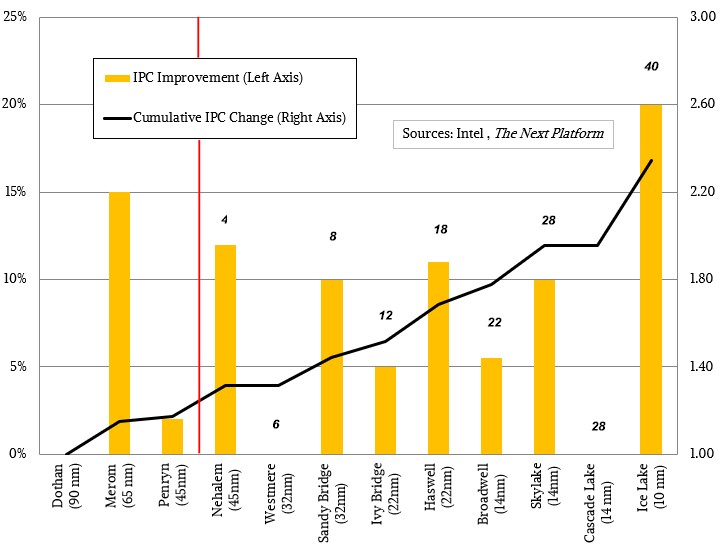 Since 2009, with the launch of “Nehalem” Xeon E5500 processors, launched in the middle of the Great Recession and blunting the Opteron server attack from AMD, manufacturing processes have shrunk by a factor of 4.5X, transistor counts on top-bin server parts have grown by 15.6X, driving core counts up by 10X and IPC rose by 2.35X cumulatively. All chips are getting hotter and clock speeds are getting slower, on average, as this all happens. This is true of Intel Xeons and Xeon SPs as well as any other family of processors. This is just physics and thermodynamics.
This last jump with Ice Lake helps close an absolutely huge gap that Intel has with AMD Epyc chips. Not completely – don’t read what we are saying wrong. AMD still makes a cheaper compute complex and wins on many benchmarks. But Intel can compensate with bundling all kinds of other things into server deals and preserve its server CPU prices and margins.
Since everyone else in the server CPU space who is still in the game has gone back to the whiteboard and redone their cores and tweaked their instruction sets to try to squeeze more and different kinds of performance out of their cores, Intel had to do this, too. The Sunny Cove cores represent about a third of the overall performance boost, and include many changes compared to the Skylake, Cascade Lake, and Cooper Lake cores that came before it.
Intel first started talking about the Sunny Cove cores in detail at the Hot Chips conference last year, and followed that up with details on the inclusion of full memory encryption and the adoption of Software Guard Extensions (SGX) security enclaves in the fall of 2020 because, well, it didn’t have any actual server processor announcements. So without further ado, let’s take another look at the Sunny Cove core:

This is a wider and deeper core with all kinds of efficiency nips and tucks compared to the prior Lake family of cores, according to Sailesh Kottapalli, a Senior Fellow at Intel and chief architect of datacenter processor architecture, who gave The Next Platform a walk-thru. On early silicon from last year, Intel was figuring that the IPC improvement from this core would be around 18 percent, but final silicon for the Sunny Cove cores implemented in the Ice Lake chips turned out to have 20 percent better IPC. This just goes to show you how difficult, even with sophisticated simulators, it is to predict the behavior of an extremely complex system.
Kottapalli said that in the past, Intel, like every other server processor maker, was interested in an architecture that would deliver the maximum throughput on the cornucopia of industry standard benchmarks. But the focus was a little different with the Sunny Cove core and the Ice Lake chip.
“For a computer architecture in the datacenter, it really needs to deliver a high throughput, but with the best responsiveness – what we think about as throughput at service level agreement,” explains Kottapalli. “And that needs to be done across a broad set of workloads and usages that are prevalent in the datacenter. In order to do that, the computer engine needs to deliver both on traditional task parallel workloads as well as on emerging data parallel workloads. And most importantly, the performance needs to scale well both within the processor and beyond, whether that’s within a node or beyond the node. The IPC improvement on the individual components of the SPEC integer tests is 20 percent, but we actually see about 30 percent on the SPEC floating point components – and on other workloads, it is even higher. We want to make sure that all workloads get good bulk performance for the right responsiveness and low latency. That is really critical, particularly for a lot more optimization at a datacenter scale. The architecture needs to achieve a higher utilization of the infrastructure. It needs to be able to handle all kinds of workloads and it needs to deliver consistent performance across multitenant usages, as well as with large scale distributed services at the best TCO.”
To make the Sunny Cove core, Intel didn’t just guess what it should do. It looked at the applications running in the datacenters of the world and found their bottlenecks and tried to fix them. (With the help of customers, we presume.) Here is a summary table of some of the tweaks to the Sunny Cove core compared to the Cascade Lake core:

It all starts with the Sunny Cove core having a front end that has higher capacity across its elements and an improved branch predictor.
“Most datacenter workloads tend to be bursty in nature because they are generally limited by memory or the latency of bandwidth, and so on,” says Kottapalli, and it is fair to say that the Lake family had some memory bandwidth and I/O bandwidth limitations compared to other architectures. “When you are actually not limited by bandwidth, you want to execute the work really fast, and so we made the processor wider and deeper, with larger structures to actually crunch through the portions where you are not limited by memory. On top of that, we made enhancements to our translation buffers as well as how we prefetch data to make sure we have the least amount of memory blocking time. And we also optimized how we operate between the dual threads of the core such that when one thread is blocked from memory, the other thread is actually able to use the entire resources of the processor to get better performance.”
The Sunny Cove core used in the Ice Lake server chips also has some tweaks that do not appear in the Sunny Cove cores used in Intel’s client device Core chips. Which includes a larger L2 cache and a second Fused Multiply Add (FMA) unit. The L2 cache helps overall throughput, and the extra FMA helps boost AXV-512 vector math throughput.
As you can see from the table above, just about every metric has been increased by about a third, sometimes more, and there is a good reason for that. With eight memory controllers instead of the six used in the Lake family, the Ice Lake Xeon has to balance all of that out or the core would just be choking on the data coming in from the memory. Or, more precisely, the memory bandwidth would be useless because CPU cores and their L1 and L2 caches only work as fast as they do, and the schedulers can only feed the threads as fast as they do. They don’t give a damn. Amdahl’s Law always prevails.
There are a bunch of new instructions in the Sunny Cove cores, which Intel has highlighted before and which deserve a second viewing, that are encapsulated in the table below:
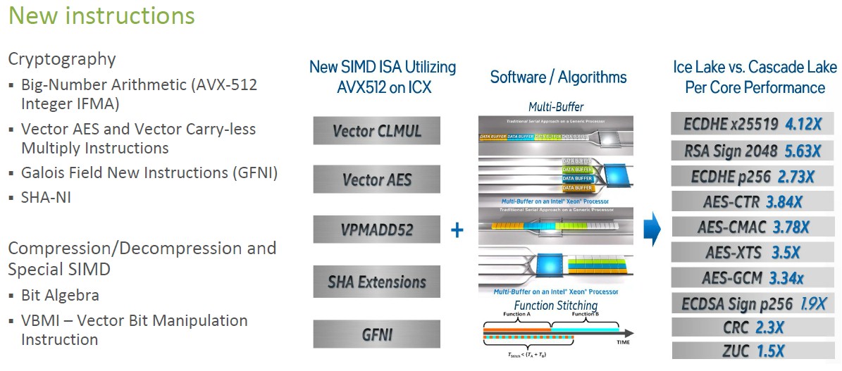
The performance improvements on cryptographic and compression/decompression algorithms from this batch of new instructions is significant, as you can see above. The pain of encrypting data is getting less and less over time. The Big Number Arithmetic (AVX 512 Integer IFMA) instruction is used for 52-bit math used in public key cryptography. Advanced Encryption Standard (AES) and its parallel compute mode (AES-GCM) are goosed, and the addition of Galois Field New Instructions can accelerate other encryption and error correction algorithms as well as bit matrix multiplication operations. Secure hashing (SHA) gets a boost, too, and the neat new one is the Vector Bit Manipulation Instruction (VBMI), which is used for accessing columnar datastores, various discrete math, dictionary-based decompression, and various data mining routines.
Which brings us to the memory and I/O subsystems in Ice Lake. The bandwidth at the knee of the latency curve is about a third better, which is about what you expect when you move from six DDR4 memory controllers to eight DDR4 memory controllers running slightly faster. (3.2 GHz, up 9 percent compared to the Cascade Lake cores). Here are the memory and I/O salient characteristics, and importantly the memory curves:

It is interesting to note that Intel is not using the STREAM Triad memory test to show the relative memory subsystem performance. We would love for Intel to actually put the memory bandwidth numbers on the charts along the X axis as it used to, and to give us STREAM Triad tests so we could compare across Xeon E5 and Xeon SP generations. Assuming these are all relative, at a knee of around 150 nanoseconds of latency, a pair of Skylake Xeon SP-8180 chips did around 230 GB/sec on STREAM Triad. Cascade Lake had a nominal improvement due to DDR4 memory speed increases, maybe somewhere around 255 GB/sec, give or take. That should put Ice Lake at around 345 GB/sec or so in a two-socket configuration at about the same latency. But as we say, real numbers would be preferable.
Kottapalli says that this was a bit trickier than just slapping down two more memory controllers, and to be able to scale well across datacenter-scale workloads, it means tweaking the memory scheduler to get the lowest latency and maximum bandwidth when the memory is operating under heavy load in a multitenant setting. The L1 cache, at 48 KB, is 50 percent bigger on the Sunny Cove core than the prior Lake cores; the L2 cache is 25 percent bigger at 1.25 MB per core, and the L3 cache is 9.1 percent bigger at 1.5 MB per core.
The interconnect and peripheral I/O is getting a boost, too, with the Ice Lake chips. The UltraPath Interconnect (UPI) links between processors with NUMA memory and processor clustering (two-socket is the only option for Ice Lake) now run at 11.2 GT/sec, 7.7 percent faster than Cascade Lake chips, and there are three links per chip to increase interconnectivity and therefore delivering a lower hop topology for such machines than earlier generations of Lake Xeon SPs that had only two UPI ports per chip. There are 64 lanes of PCI-Express 4.0 peripheral connectivity on each Ice Lake Xeon SP socket, compared to 48 lanes of PCI-Express 3.0 connectivity for the Cascade Lake chips, which is a factor of 2.7X increase in aggregate peak bandwidth.
While those aggregates in capacity and bandwidth for different parts of the processor are always important, it is the tail latencies on real applications that Intel is focused on killing, which Kottapalli alluded to. And interestingly, he gave us a chart that shows what he is talking about. Take a look:
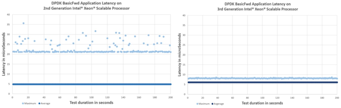
Architecture is always about pushing the limits and making compromises. Data plane forwarding is a very tough workload, and frankly one that is necessary for software-defined networking and one that CPUs have historically been very poor at doing. Some companies hate the high cost of networking appliances enough to replace them with a bank of X86 servers running software and have been willing to wait for Moore’s Law to bring the hardware footprint down. But those tail latencies are absolutely killer, as the chart above on the left shows running on a Cascade Lake Xeon SP running the BasicFwd application using Intel’s DPDK. But with some tweaks to the architecture that, as you can see, allowed the average latency to rise a bit – you can barely perceive it at maybe an incremental nanosecond or two, but in percent it would look big –the tail latencies come way, way down and are more deterministic.
As we have pointed out many times, predictable latency is a lot more important for distributed applications than the absolute lowest latency. It will be interesting to see how various workloads make use of these architectural differences. And that is why we will be doing an analysis of Ice Lake Xeon SP performance compared to its predecessors next. Stay tuned for that.
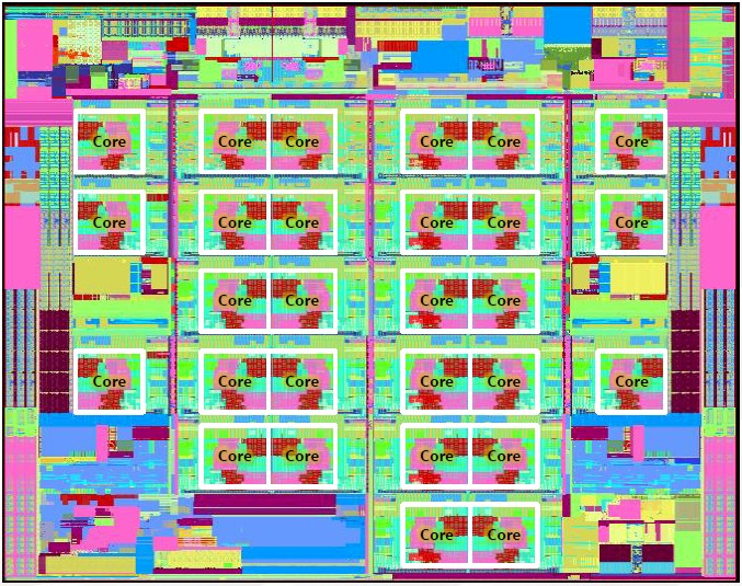
But before we leave, one last thing. Intel is not giving out block diagrams of the Ice Lake dies, of which we think there are probably four. The 10-core LCC, the 18-core HCC, the 28-core XCC, and what we are calling the 40-core UCC, short for low, high, extreme, and ultra core counts. Here is the 28-core die shot that we do have for Ice Lake:
And here is the 28-core block diagram:

And finally, here is the 40-core block diagram:
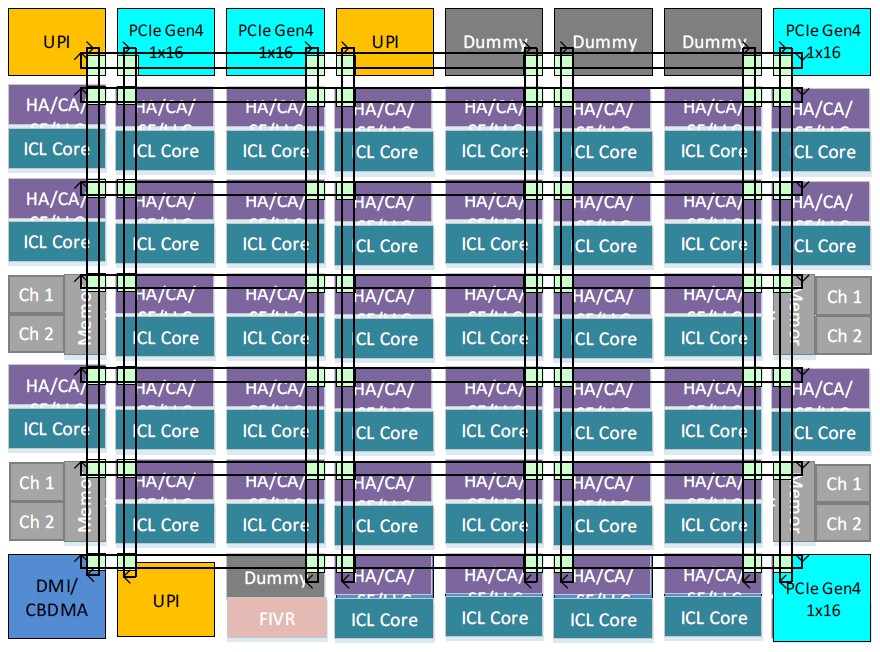
That’s all we could find. Intel is being cagey for reasons we do not understand. It happens that way sometimes.

Another Crazy Idea: Intel Might Buy Globalfoundries
Back in March, when we wrote up Intel’s Integrated Device Manufacturing 2.0 strategy put forth in the vaguest of terms by then-new chief executive officer Pat Gelsinger, we quipped that Intel might be wishing as it launches Intel Foundry Services that it had some of its older fabs around with …
Ampere Aims For The Clouds With Altra Arm Server Chip
At this point in the history of information technology, there is no way to introduce a new processor that does not appeal to the hyperscalers and cloud builders. But it is another thing entirely to design a chip aimed only at these customers. And that is precisely what Ampere Computing, …

The Impending AMD Milan Versus Intel Ice Lake Server Showdown
What a strange server CPU world we live in. The dozen or so biggest customers in the world command something on the order of 45 percent of the server CPU shipments, but significantly lower share of the revenue because of the volume discounts they can command, and they not only …
Excellent article!
I really enjoyed reading this, and look forward to updates on the real-world tests.
In my line of work, having increased intra-core memory and predictable latency have the most impact on performance when running simulations on multiple nodes that each have multiple CPU sockets and GPU’s.