

At this point in the history of information technology, there is no way to introduce a new processor that does not appeal to the hyperscalers and cloud builders. But it is another thing entirely to design a chip aimed only at these customers.
And that is precisely what Ampere Computing, the upstart Arm server chip maker headed by former Intel president Renee James and backed by the big checkbook of private equity firm The Carlyle Group, says that it is doing with its “Quicksilver” Altra line of processors, which are being branded and unveiled more fully today.
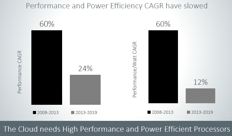
The resurgent AMD has largely been able to get a toehold once again in the datacenter because its Epyc server chips were designed to address the specific needs of these hyperscaler and cloud builder customers, and therefore have a chance to ramp faster because of the large number of servers that these companies install each year. It is widely believed that chip maker Qualcomm was enticed to enter the Arm server fray several years ago with its Centriq line of chips with the encouragement and support of Google, which has also backed IBM’s Power processors through the OpenPower Foundation as a means of keeping pressure on Intel, which has essentially owned datacenter compute for the past decade and which ahs the gross margins to prove it. Qualcomm, like Broadcom and Samsung before it, had other and bigger fish to fry and exited the Arm server business in May 2018, leaving Marvell the dominant supplier of Arm chips for datacenter compute with its ThunderX2 line. But it has been several years since these chips were updated, but as we reported in December, there is a ThunderX2, based on 7 nanometer manufacturing processes, in the wings for 2020 and it looks like Marvell will be on a two year cadence. Amazon Web Services looks to be on an annual cadence with its homegrown “Graviton” server chips, and any speculation that Ampere Computing had AWS lined up as a potential server customer – the prior brand on the “Skylark” line of X-Gene 3 chips it got when it acquired the X-Gene intellectual property created by true Arm server chip upstart Applied Micro – is just idle talk. For now. (Those chips were branded eMAG, which could have been short for “Microsoft Amazon Google” or “Microsoft Alibaba Google.”)
Ampere Computing – we have to use its full name not to confound search engines when Nvidia releases its “Ampere” generation of GPU engines – is going to be on a much tighter cadence, getting back to an annual rhythm of updates that was the norm in the computer business for many years and that Intel let slip as its competitors were vanquished from the glass house and, quite frankly, allowed it to coast quite a bit and still rake in the money. Face it: You would have done the same thing as Intel if it was you. Server chip makers have been chasing Intel since the Great Recession faded in 2010, and only now is Intel feeling the burn bad enough that it has to rejigger the “Cascade Lake” Xeon SP line to make a price cut look like a revamp.
We are not going to get into the whole history of Ampere Computing today, but a small review is in order. The company was set up in the spring of 2018 to chase the hyperscalers and cloud builders, and by the wall the Skylark chips, which were a tweak on the existing X-Gene 3 designs, were getting into the hands of early customers. As 2019 was winding down, we touched base with Ampere Computing to get a sense of where the next-gen Quicksilver processors were at and what the future roadmap looked like, and today, the Quicksilver chip is being given its Altra brand name and the feeds and speeds – as well as the design philosophy – of this and future Altra chips beyond the Quicksilver device are being divulged.
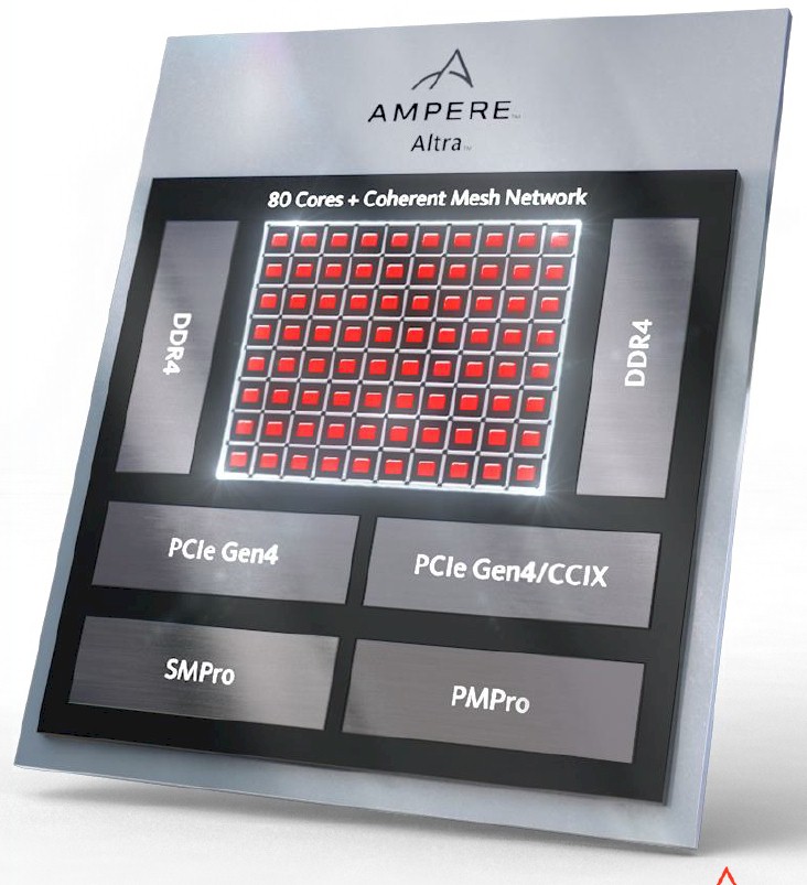
We already knew that the Quicksilver chip was going to have 80 cores – that’s a big number – and was not going to use a variant of the homegrown X-Gene core created by Applied Micro and tweaked by Ampere Computing for the eMAG 1 chip, but would rather be based on the “Ares” cores used in Arm Holding’s Neoverse N1 platform. The Quicksilver chip uses Ampere’s own mesh interconnect for on-die communication, and it is a monolithic die rather than a chiplet design that will be etched in the 7 nanometer processes created by fab partner Taiwan Semiconductor Manufacturing Corp.
AMD has a PC chip business, so it is no surprise that it would be on the front end of chiplet designs that gang up multiple chips inside of a socket. But there are some penalties to be paid in terms of latencies across the dies and the complexity of making the package.
“I think the vectors of that decision about chiplets versus monolithic falls into two buckets,” explains James tells The Next Platform. “One is cost, and if you allow cost to lead you might end up in the wrong place. The other one is performance, and if you are careful with your design and performance is your objective, you would hang with monolithic as long as you can – knowing that you can’t forever. The way that you disaggregate is almost as important as the decision to disaggregate. Not all chiplets are made the same and with a lot of the designs, the way that people are disaggregating may not end up allowing the scalability and performance that is required. So then you have to redesign. Coming from a background of monolithic, you would expect the team at Ampere to be efficient designers and that performance was our high order bit. We understood the need to disaggregate and we have a multi-chip roadmap, but we want to be smart about it and not rush it. And I think given the performance of the Altra chip and the health of the tape out, I feel like that ended up being a wise decision. And it wasn’t an obvious decision in the face of AMD and in the face of what people were saying in the industry. It sounded scary when we went down the path.”
The good news is that if Ampere Computing can get higher performance as well as deterministic performance, it can charge a premium for that – or at least more than it might have otherwise been able to.
The stock Ares N1 core has 64 KB of four-way L1 instruction cache and 64 KB of four-way L1 data cache and a private L2 cache that comes in either 512 KB or 1 MB flavors. That N1 core has a four-wide front end with an instruction pipeline with eleven stages, and includes three 64-bit integer units and a pair of 128-bit SIMD units. Technically speaking, it is a superscalar microarchitecture that has out of order execution baked in – a very standard RISC processor in many ways. The integer units support 8-bit INT8 instructions and the SIMD units support half precision or 16-bit FP16 floating point instructions, which are both important for machine learning inference workloads. Jeff Wittich, senior vice president of products at Ampere, says that Ampere Computing has support for Google’s bfloat16 variant of FP16 in the works on future processors. Arm Holdings added bfloat16 to its architecture last September, and it will take time to implement.
That eleven stage pipeline can access the 1 MB L2 cache, and if you use the 512 KB L2 cache, the pipeline drops back to nine stages to balance it all out. Ampere Computing is using the deeper pipeline with the 1 MB L2 cache. Those private caches are linked directly to the cores and help drive the per-core performance up, according to Wittich. Ampere Computing is wrapping a 32 MB L3 cache around the whole shebang, although it is not clear how that cache is being implemented – across that mesh in a highly distributed fashion or on the edges of the mesh in a segmented fashion with bigger blocks.
“There is a need for predictable high performance for the modern cloud, to provide scalability across the platform – cores, memory, I/O, everything – and we need power efficiency and density,” explains Wittich. “We are focused on integer performance, high core count, large caches, very strong quality of service, high I/O and memory bandwidth, and all so we would be, you know, the perfect choice for deploying anything in containers, as a microservice, as a function – the way that things get deployed today in the cloud, which is very different than running one big monolithic application in an enterprise datacenter. Single threaded cores are so important from a performance perspective, and they provide greater isolation and a smaller attack surface.”
The architecture of the Quicksilver core is at the Armv8.2+ level, and that plus means Ampere Computing is pulling some of the features from the Armv8.3 and Armv8.4 in, with those mitigations being just one example. The one thing that the Quicksilver chips do not have – and that Ampere Computing does not seem to be interested in at all – is support for simultaneous multithreading, or SMT. And while hyperthreading, as it is commonly called after the Intel flavor of SMT, has some benefits in driving efficiencies, it also carries a cost and that is that performance is inherently less deterministic across two or more virtual threads than across a bunch of cores implementing one thread each.
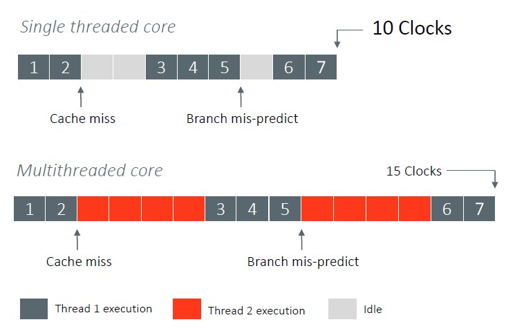
Ampere Computing is big on cores as threads because it eliminates those noisy neighbor problems that make instruction execution for specific threads take longer when examined at a thread basis. Yes, you might be able to get 20 percent or 30 percent more work pushed through the machine with SMT2 (two threads per core) or SMT4 (four threads per core) turned on, but each bit of work takes longer to complete and it is also harder to predict when it will complete each time it runs because other work interferes.
“We have ensured that all cores can run at the same sustained turbo frequency because while there might be times when it makes sense to run clocks very high on a single core when 90 percent of your CPU is idle, that’s not how the clouds typically run,” explains Wittich. “If 90 percent of your CPU is idle, you’ve got a problem and something’s wrong with the way you are operating. And if it is just an intermediate state where for a few minutes your server is mostly idle, you don’t really want to push the frequency up because minutes later, when you bring in all the other users onto that box, you don’t want the frequency to then drop. Then, users can’t figure out why the frequency keeps bouncing around. One minute their application ran great, and the next minute their application has high latency. So are focusing on delivering all the performance to every user at all times.”
The first generation Altra processors are designed to run at 3 GHz in an all-core Turbo mode, and it does not implement a higher single-core Turbo mode like Intel does with its Xeon SP processors. And all core Turbo mode is the same thing as saying there is no Turbo mode, as we know it at least, and Wittich says that there is thermal room to jack the clocks up to 3.3 GHz if customers need it, so that is akin to a Turbo mode if you want to think about it that way. Depending on the number of cores activated, the Quicksilver chips will span from 45 watts (with maybe 10 cores) to 200 watts (with the 80 cores).
No SKUing The Customer
The Quicksilver chip has eight memory channels, as we have said before, but we now know that the eight memory controllers will support 3.2 GHz memory speeds and that the Quicksilver chip will allow four, six, or eight memory controllers to be activated as needed. The memory controllers support one or two DIMMs per channel, as needed, and support memory sticks with four or eight banks based on either 8 Gb or 16 Gb memory chips. The controllers also support DRAM throttling to restrict data traffic on the memory bus to lower its heat dissipation (and therefore its performance) as needed for thermal reasons inside of the server, and the memory controllers are linked to the outside of the internal Altra mesh interconnect in such a away that memory latencies across that mesh between any cores on the die are as consistent as possible. With all eight memory controllers fired up, a Quicksilver socket can push 200 GB/sec of memory bandwidth per socket – that is about what a two-socket Xeon SP server can do, which only has six memory controllers. Up to 4 TB of memory per socket is supported. This is some fat and fast memory, indeed.
Each Quicksilver chip has two PCI-Express 4.0 controllers, delivering a total of 128 lanes of connectivity. When two processors are linked NUMA style to share memory, 64 of the combined lanes (32 from each chip) are burned to do the NUMA connection, but 192 lanes are left over to handle peripheral I/O. One of those PCI-Express controllers can connect up to four devices (each with 16 lanes) using the CCIX protocol spearheaded by Xilinx and adopted by Arm as its NUMA interconnect. We strongly suspect that the CCIX links can be used for NUMA or for accelerators at the same time, but obviously with half as many CCIX x16 ports left over if two of them are burned making the NUMA links between two chips. The x16 lanes on the controllers can be broken down into x8, x4, and x2 lanes, as you would expect, and all lanes are available across all SKUs in the Quicksilver line. Ditto for memory controller options and memory access.
“All of our processor SKUs will support all of the I/O and all of the memory,” says Wittich. “We don’t do I/O SKUing or memory capacity SKUing , and we want to put the capacity choices in the hands of customers so they can go and innovate.”
The last two blocks on the Quicksilver Altra diagram are the PM Pro and SM Pro control processors, which adhere to the Server Base System Architecture Level 4 specification from Arm Holdings and which manage the servers, provide secure boot, do RAS error reporting, and do power management and temperature control.
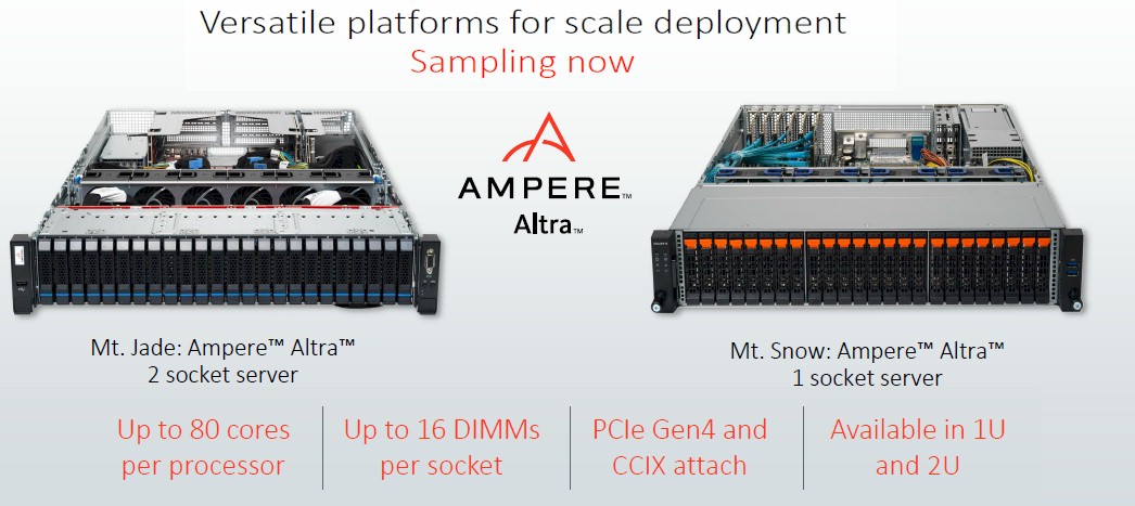
The Quicksilver Altra chips are sampling now to key hyperscaler and cloud builder customers, and Ampere Computing has cooked up two platforms – a single-socket server and a two-socket server – that customers can use as a development and test platform. Here they are:
That leaves on three more things, and the important ones for any upstart trying to get credibility in the server chip space: The roadmap for future chips, the performance benchmarks for the current chips, and the prices for chips. We will be covering the performance of the Quicksilver chips separately, we have no idea about pricing yet, but here is the latest roadmap from Ampere Computing:
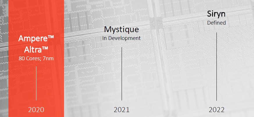
This is very similar to the roadmap that was shown to us in December, except that the future two chips now have names and the manufacturing processes have been removed from the charts. But the “Mystique” chip will be made on a rev of the 7 nanometer process when it launches in 2021 and the “Siryn” chip will use 5 nanometer processes when it comes out in 2022. These are about a year after Arm will ship its “Zeus” and “Poseidon” chip designs and their respective cores, as you can see from the Neoverse roadmap.
The Mystique chip will include Arm cores that have been more substantially tweaked than the N1 cores uses in the Quicksilver chips, but it is not clear how as yet, and we expect that the Mystique chip will be socket compatible with the Quicksilver chip so server makers don’t have to reinvent the socket and motherboard. Out guess is that Siryn will be a different socket, possibly one supporting both DDR5 memory and PCI-Express 5.0 peripherals. It is hard to say when Ampere Computing will shift from monolithic to chiplet designs, but our guess is that will happen along with the shrink to 5 nanometers, with perhaps I/O and memory controllers staying at 7 nanometers while the cores and other elements shrink to 5 nanometers. Time will tell.

Cisco: Datacenter Demand Strong, Supply Not So Much
The good news, and we all need to be looking at the bright sides of things a bit these days is that the biggest IT shops in the world want to buy a lot of datacenter gear from Cisco Systems. Across the board with large enterprise and commercial accounts, the …
How Long Before AI Servers Take Over The Market?
When hyperscalers and cloud builders think about their infrastructure, they talk about megawatts and they think about the mix of serving and storage and the total capacity that is delivered in a megawatt of power. And of course they also think in terms of budgets because money is, in fact, …

Server And Storage Spending Growth Looks Rosy Out To 2027
For a market that is so integral to the global economy, it sure is hard to get a complete dataset on quarterly and annual spending on information technology. We try to gather up all of the information we can find and flesh it out where we can so you can …
“simultaneous hyperthreading.”
Hyper-Threading is Intel’s marketing branding for Intel’s version of SMT(Simultaneous Multi-Threading) so please fix that. Now onto those 80 cores non SMT based cores is that the pipeline bubbles will become numerous if that branch perdition logic does not make the right choices as often as possible.
There is going to have to be a greater amount of time focused on code/compiler optimization in an effort to get around that having no SMT but for the workloads that can be better optimized for less unpredictability than that’s not as bad.
There’s still one thing that concerns me about the potential for ARM servers either in the public cloud or the datacenter: the need for a consistent server architecture, not just a standard CPU. If I build an application for Linux on x86 I can expect that it will run more or less equally well on any x86 vendor’s systems, and probably require only minimal changes between Linux distros. With an ARM server, is there an equivalent? Or do I have to design / optimize / test my application uniquely for different memory architectures, I/O designs, etc., on Ampere’s systems, AWS’s systems, ThunderX2-based systems… even assuming that the different ARM CPUs involved are instruction set compatible and I don’t have to recompile (or use RPLs for missing instructions) on every CPU?
Without that level of compatibility, it’s going to be tough to achieve critical mass for ARM servers as a target market, and therefore to attract software whether infrastructure (frameworks, libraries, …) or apps themselves.
Jacob is spot on. With so many different implementations of ARM cores where licensees are free to [not] implement optional instructions and then also have unique extensions, it makes it a nightmare for ISVs to support and they end up coding to the lowest common denominator potentially leaving a ton of headroom in performance on the table. Big name ISVs won’t optimize for you unless you throw a ton of money at them.