

It has been a long time since Intel changed its manufacturing process – what it used to call a “tick” – and the microarchitecture and architecture of a processor design – what it used to call a “tock” – at the same time. But with the fourth generation “Ice Lake” Xeon SP processors that were unveiled to a certain extent today at the Hot Chips 32 conference, Intel is doing both at the same time.
Whether or not this was the plan is moot, and frankly, it is not worth the time to reassemble the torn up Xeon server processor roadmaps and tape them back together, much less to lament the several big delays in rolling out 10 nanometer manufacturing processes for any server CPU. Ice Lake is being revealed and no matter what, it is an improvement over the current second generation “Cascade Lake” and third generation “Cooper Lake” Xeon SP processors, and importantly gets the new “Sunny Cove” core, which has very substantial performance improvements over the cores used in both of these processors, which aside from some tweaks here and there (including support for Bfloat16 math), are essentially the same and only offered modest tweaks over the “Skylake” cores used in the first generation Xeon SPs.
From a technical standpoint as well as for manufacturing prowess bragging rights, it would have been better for Intel had 10 nanometer etching been available years ago and something like Ice Lake was available to make use of it. But, as it is, the 14 nanometer holding pattern that Intel has been stuck in with the Xeon SPs has left just enough room for the competitive camels to get their noses under the circus tent and perhaps get inside. We doubt very much that any of them – AMD, IBM, Ampere Computing, Marvell and upstarts like Tachyum or Nuvia – can bring the tent down. If the repeated delays of 10 nanometer and the more recent push out of 7 nanometer manufacturing have not collapsed the revenue and profit engine that is the Xeon SP within the Data Center Group, it is hard to imagine what might bring that tent down.
As it is, Ice Lake will be the pole that Intel can finally deploy to make its tent stronger and perfect the yields on the 10 nanometer processes so that next year’s fifth generation Xeon SP, code-named “Sapphire Rapids” because Intel is tired of jumping in the lake, can act like camel repellent, and hopefully strong enough so that the gap to the sixth generation 7 nanometer “Granite Rapids” Xeon SPs, now due in the first half of 2023, does not leave more room for the competitive camels to get their necks as well as their noses under the circus tent.
The wonder is not that Intel is having such troubles – all big tech companies sometimes bet big and lose big, and the tick-tock methodology invented by Pat Gelsinger, formerly in charge of the Data Center Group many years back and happily installed as chief executive officer of VMware before Intel started having woes, was designed explicitly to mitigate against such risks. The trouble is, what do you do when the clock stops ticking and can only go tock? The short answer is you take a hard look at your foundry operations and then you tap a rival for some of the work, which drives up costs and drives down profits but it eliminates some risk.
It is against all of this backdrop that the Ice Lake Xeons are being revealed, and given the relatively short life that they will have and very likely lower profit margins because of higher 10 nanometer manufacturing costs and much more intense competition, we suspect that Intel’s expectations are to see a dip in profits in Data Center Group in the coming quarters even if it does manage to keep revenues growing. We shall see what price points and risk level the server chip market will bear. The time is ripe for change, that is all we know.
As far as we can tell, Intel’s processor designers do not suffer from a shortage of ideas on how to improve Xeon SP processors. The changes made in Ice Lake demonstrate this aptly. They just need process shrinks to help pay for the transistor budget required to implement them. And in that regard, the – finally! – shrink from 14 nanometers to 10 nanometers is going to help and so will the tock of the Sunny Cove cores and architecture tweaks around them that make the Ice Lake chip a whole lot more relevant than the Cooper Lake Xeon SPs that launched only on big iron in June and did not make it to little iron at all, thus leaving room for Ice Lake. It’s as if we have the Xeon E5 and Xeon E7 split again, but only for this intermission. We think. Maybe. We shall see.
Skating Along On Ice Lake
While the cores in the Ice Lake processor are different from those used in the Skylake through Cooper Lake processors, Irma Esmer Papazian, senior principal engineer in architecture at Intel who gave the presentation at Hot Chips, explained that the mesh fabric, the compute tiles, and the distributed L3 cache memory for the earlier Xeon SPs and the impending one were all quite similar. In a sense, at least from the presentation today, Ice Lake is a 10 nanometer shrink with a global replace of the Skylake cores with the Sunny Cove cores, with the typical tweaks throughout the architecture, of course, that come with any update. The core and uncore layout is a bit different, for reasons Esmer Papazian explained.
Take a look at Ice Lake’s die shot for a 28-core variant:

It looks a bit less compact in some ways than Cascade Lake, which is obvious when you look at the block diagrams side-by-side for Cascade Lake and Ice Lake:
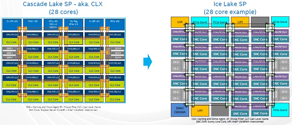
The cores have caching and home agents on top of them to talk to the mesh interconnect that links all of the elements of the die together as well as the L3 cache segments that are unified for all of the cores by that mesh. There are two blocks of three memory controllers, left and right, on the Cascade Lake chip, and the I/O such as PCI-Express and UltraPath Interconnect (UPI) controllers run across the top.
There are a couple of things to note here. First, this is the Extreme Core Count, or XCC variant, of the Cascade Lake design, which like the Skylake through Cooper Lake chips, has 28 cores. There is also the High Core Count, or HCC, variant, with 18 cores and a different layout and die size, and an even smaller Low Core Count, or LCC, variant that has 10 cores. So, there are actually three Xeon SP chips, not one, in each generation up until now. Intel is not preannouncing the Ice Lake lineup – that comes later – and specifically did not say if the 28-core version of Ice Lake was the HCC or XCC variant. Don’t assume anything. With 10 nanometer yields being what they are, there is a good chance that Intel will try to limit the die variations and just block off the unusable chunks and go with maybe two designs, perhaps one with 18 cores and another with 28 cores. It’s hard to say.
What we can see is what Esmer Papazian pointed out, and that is the 28-core Ice Lake part was rejiggered to increase the outside edging on the die and to spread controllers out around that edging both top and bottom. The DMI and CBDMA controllers were broken free of the PCI-Express controller (they were linked with Cascade Lake and prior Xeon SP chips), and now there are four PCI-Express 4.0 controllers with Ice Lake as well as that separate DMI/CBDMA controller. The Cascade Lake chip had three UPI links, and as far as this block diagram shows, Ice Lake has three as well. But what indeed are the two gray boxes, one on the north side and one on the south side?
Well, they could be extra UPI controllers that are blanked out because they are no longer needed for either putting two chips in a single socket or for creating more tightly coupled four-way and eight-way – and possibly even sixteen-way – NUMA systems. Ice Lake is only being delivered for two-socket “Whitley” server platforms from Intel, so the extra UPI links are not necessary. Or they may be activated if Intel does dual chip module (DCM) implementations to boost sockets to 56 cores.
If you put a gun to our heads, we would have said the two gray boxes are UPI links, not cores, and that Intel will indeed deliver DCMs as it did with the Cascade Lake-AP variants last year. We could be wrong. These could also be spare cores or spare PCI-Express controllers to help increase chip yield. But we think this is unlikely. More UPI ports would be most useful, but then again, so would 96 PCI-Express lanes per socket. So, with the gun cocked, we will say one gray box is UPI and the other is PCI-Express, for a total of 80 lanes per socket for external I/O and 80 lanes of UPI for interconnect either across sockets or within them.
With the advanced power gating and telemetry that is part of the Ice Lake design, turning things on and off is a lot easier with the Ice Lake design than it is for prior Xeon SPs, and we think Intel will only roll out the HCC and XCC variants. We think there will be DCMs based on both the HCC and XCC variants. There is not much of a point in creating a DCM based on the LCC, if there is one. At that point, LCC admirers should just use Cascade Lake since their processing needs are obviously small.
Aside from the small core count of the prior three generations of Xeon SPs relative to the processors others have brought out or are bringing out, the biggest Achilles heel for these Intel server chips has been the limited number of memory controllers in these devices. With the Ice Lake Xeon SPs, this is being fixed, and with a ground up redesign of the memory controller. There are a lot of tweaks, but the memory bandwidth improvement is largely done through speeding up the memory and adding more memory channels; that said, only about 45 percent of that bandwidth improvement comes from these factors in the chart below, which shows STREAM Triad benchmark results for Cascade Lake versus Ice Lake:
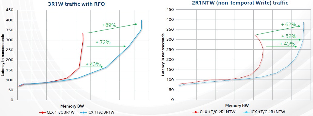
Intel is obviously obfuscating the bandwidth numbers on the X axis. A two-socket Cascade Lake-AP (which is four processors using a pair of DCMs) topped out around 400 GB/sec on Stream Triad, or about 100 GB/sec per processor. So those X axis squares should be around 50 GB/sec for a two-socket SCM machine. Call it somewhere around 150 GB/sec per socket, with most of that coming from the additional 33 percent in memory bandwidth and another 12 percent coming from increased memory clock speed. The important thing is to see how much better the Ice Lake curves behave, especially with non-temporal write traffic.
The Ice Lake memory controllers also include what Intel calls Total Memory Encryption, or TME, which encrypts all data in memory using the 128-bit AES-XTS protocol. The encryption key for memory is stored in the processor and is not accessible through software (even Intel can’t do it) and it is enabled in the system BIOS. Esmer Papazian said that the goal was to keep the performance penalty hit to 5 percent or lower when using memory encryption, but that on pre-production silicon coming back from the fabs, the performance hit was somewhere between 1 percent and 2 percent, depending on the nature of the data and workload on the system. It is important to note that AMD broke this ground of memory encryption with the “Rome” Epyc processors, and that IBM is following suit with its Power10 chips due in the fall next year (as we learned today).
The PCI-Express 4.0 controllers on the chip, which would have been cutting edge had Ice Lake come to market on time, run at the same frequency as the uncore now (2X that on Cascade Lake) and have new I/I virtualization features that have a lot more bandwidth and that allow for virtual machines to run at near-native performance if they are using large page sizes.
That leaves the Sunny Cove core itself that is embedded in the Ice Lake design, and it is an important feature indeed. Let’s take a look at the core microarchitecture as Esmer Papazian revealed it for the Xeon SP server chips:
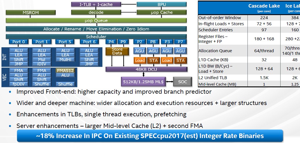
This is a much wider and deeper core, and just about everything has been tweaked to be more efficient as well as to yield more throughput. On pre-production silicon, the Sunny Cove core, normalized to the same frequency, is yielding around an 18 percent instructions per clock (IPC) improvement over the Cascade Lake and Cooper Lake cores. This is the largest leap in IPC that we have seen from Intel in a long, long time. And it is equivalent to adding around five cores to a Cascade Lake or Cooper Lake Xeon SP at the same clock speed.
Moreover, the AVX-512 vector math units have been tweaked to have a finer-grained clock speed downshift when under load so the performance hit is not so bad – good news for those who are using AVX-512 to math up floating point and integer data.
The Sunny Cove cores have a slew of new instructions:
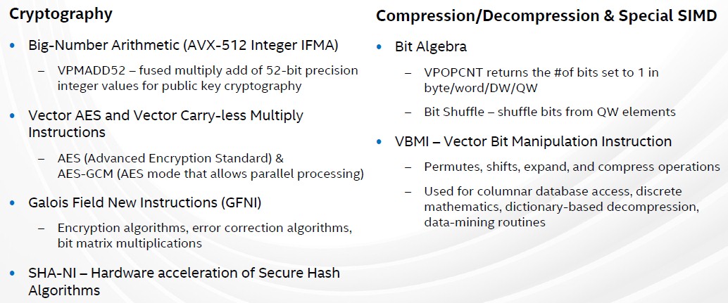
The focus areas for the Hot Chips talk were for cryptography and data compression, and depending on the software and algorithms and the accelerators and instructions used, per core performance on this work ranges from 1.5X to 8X better on Ice Lake than on Cascade Lake and Cooper Lake.

Stacking Up Intel Gaudi Against Nvidia GPUs For AI
Updated: Here is something we don’t see much anymore when it comes to AI systems: list prices for the accelerators and the base motherboards that glue a bunch of them together into a shared compute complex. But at the recent Computex IT conference in Taipei, Taiwan, Intel, which is desperate …

CXL And Gen-Z Iron Out A Coherent Interconnect Strategy
To one way of looking at it, a reprise of the Bus Wars from days gone by in the late 1980s and early 1990s would have been a lot of fun. The fighting among vendors to create standards that they controlled ultimately resulted in the creation of the PCI-X and …
3D XPoint Memory At The Crossroads
Like many system architects the world over, we had high hopes for the 3D XPoint variant of phase change memory (PCM) when it launched with much fanfare back in July 2015 after being developed jointly by Intel and Micron Technology for many, many years. This represented a new kind of …
I watched most of the sc20 videos from Intel. Some mentioned this Ice Lake Server chip. I didn’t see much about the avx512 enhancements or pcie4, but there were several customers talking about use of Optane DIMMs in their systems.
I wonder if the Optane DIMM advantage trumps any delays in 7nm processing, especially now that AMD’s pcie4 advantage is disappearing.
Intel also announced that Sapphire Rapids is “broadly sampling”. That adds pcie5, AMX, CXL, avx512 bfloat16, DDR5 capabilities out there being evaluated, along with a new 10ESF process and new core architecture.