
At long last, Intel is finally shipping a Xeon SP processor that is based on a 10 nanometer chip manufacturing process and it is finally able to do a better job competing on the technical and economic merits of its Xeon SP processors as architected rather than playing the total system card or the risk card or the discount card to keep its core datacenter compute engine business humming along.
Despite all of the woes, provided that Intel can make enough of them using its still-maturing 10 nanometer process, Intel can stand toe to toe against AMD’s Epycs, Ampere Computing’s Altras, and IBM’s Power9 and maybe even its future Power10. For the past several years as it awaited the much-delayed 10 nanometer process, which had to be scrapped and started all over from the beginning, Intel had no choice but to rejuggle the chip bins, find those chips that run a little faster thanks to the maturity of its 14 nanometer process, add a core or two to each rejiggered SKU, and slap some (slightly) lower price stickers on them.
That is essentially what happened with the “Cascade Lake” Xeon SP launch in 2019 and the “Cascade Lake-R” refresh in 2020 that followed the “Skylake” Xeon SP rollout in 2017. And Intel would probably prefer that no one mention the 400-watt, 56-core “Cascade Lake-AP” dual-chip module that was said to “compete” with AMD’s 64-core “Rome” Epyc 7002 processors. That word “compete” is in quotes for a reason, and that is because on the technical merits and economics, AMD was smacking Intel around pretty hard throughout this time. But you wouldn’t know it from Intel’s sales figures for its Data Center Group because Intel focused on a system sale, which means in essence that Intel can create a bundle of CPUs and chipsets, and Optane memory, and network interface cards and maybe even motherboards or whole systems and maybe for a few companies (like Microsoft) a whole bunch of FPGAs and allocate revenue as it sees fit in the bundle. In other words, it can discount like hell on all the extra components and make it look like it doesn’t have to cut CPU prices. Of course Intel has actually cut its CPU prices in the past three years due to competitive pressure, especially given the price/performance advantage that AMD has been able to show at the CPU-level with the Rome and now the “Milan” Epyc 7003s, which launched in mid-March. (We are still working on a review of the competitive landscape for Milan as AMD sees it.) Try to prove it, though. Good luck with that.
Our point is, the bin juggling game is over now unless 10 nanometer manufacturing hits a snag. (Intel has already sold over 200,000 units of the Ice Lake Xeon SP since they went into production in December 2020 and volumes are ramping.) You can rest assured that Intel is going to keep playing that system trump card, again and again and again.
On the tech front, Intel doesn’t have to bin juggle any more. The company has new “Sunny Cove” cores that are delivering 20 percent improvements in instructions per clock (IPC), a gauge of raw integer performance, over the cores used in Skylake and Cascade Lake processors; the slightly tweaked core used in the 14 nanometer “Cooper Lake” Xeon SP processors, which debuted last June, are essentially the same cores but sporting the Bfloat16 data format for vector processing created by Google and, importantly, also used by Facebook for their machine learning algorithms. The Cooper Lake Xeon SPs are restricted to machines with four or eight sockets and have six UPI links running at 10.4 GT/sec. The Ice Lake Xeon SPs are restricted to machines with one or two sockets, and that is an important distinction compared to the prior Skylake and Cascade Lake generations. Intel’s delays with 10 nanometer manufacturing messed up its product SKUs and roadmaps, and we presume that when the “Sapphire Rapids” Xeon SPs launch sometime in 2022 with a tweaked SuperFIN variant of the 10 nanometer process, we will return to one chip generation spanning all socket configurations, as has been the case for several years now.
Like IBM with Power10 and to a certain extent with AMD’s “Zen 3” cores in the Milan Epyc 7003s, Intel has to go back to the whiteboard on the cores, which it has done from time to time in its history, to either drive energy efficiency or performance or both. The IPC jump is, at 20 percent more oomph per clock cycle than the Skylake/Cascade Lake/Cooper Lake core, a pretty big jump for Intel. In fact, it is the biggest one that we have seen in recent years:
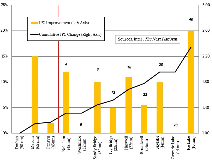
It is the interplay of shrinking processes, architectural changes that drive IPC and core counts, and clock speeds that allows for more transistors on a die to turn into more performance, and this chart shows the increases in IPC and core counts since the mobile cores created in Intel’s Israeli labs and fabs were adopted by necessity when the prior generations of Xeon CPUs were getting their clocks cleaned by AMD chips on energy efficiency, core count, throughput performance, and memory bandwidth.
In a past life at the chip maker, Intel’s newly anointed chief executive officer, Pat Gelsinger, invented the tick-tock method of chip production, splitting manufacturing process innovations from architectural changes and thereby minimizing risks for each successive generation of Core or Xeon processor. This was not the original plan, of course, but the Ice Lake Xeon SP involves both the tick of process shrink and the tock of a new core design at the same time. But Intel could not deliver a new core without a new process – everything that could have been done in 14 nanometers and still stay in a reasonable power envelope was done with Cascade Lake and Cooper Lake – and for a while it could not deliver a new process. That 10 nanometer conundrum was a big freaking problem, and to be fair, Intel has played its hand about as well as anyone could. And it would have been far, far worse if Intel did not have what amounts to a monopoly in datacenter compute, the inertia of customers, and the bundle game to help it bridge this enormous gap.
The chart above puts the IPC improvement with the Sunny Cove cores into perspective. The vertical red line separates mobile processor cores and their IPC improvements generation to generation from the server CPU cores starting with “Nehalem” in 2009 all the way up through Ice Lake today. The cumulative IPC is reckoned against the “Dothan” core launched in 2004 in the Celeron M and Pentium M, which were etched using 90 nanometer processes. The Merom cores were still ticking and tocking at the same time, to a certain extent, with a process shrink and a big change in process down to 65 nanometer processes. The Penryn cores were more of a tick, with hardly any IPC improvement and a shrink to 45 nanometers, and the Nehalem cores, which were made in 45 nanometers as well, were a tock with substantial IPC improvements in the core as well as a doubling up of cores as Intel was able to make larger chips and get yields.
We like to gauge things in the server business since the Nehalem Xeon E5500 launch in March 2009, which is when Intel got the upper hand back from AMD’s Opteron in the middle of the Great Recession, where server makers and server buyers were in no mood to take on any unnecessary risk and set AMD on a path of abandoning the server business for five years before roaring back into it with the “Naples” Epyc 7001 processors in June 2017. (Was that really four years ago?)
Since that time, Intel has dropped from 45 nanometer to 10 nanometer processes, which is a 78 percent decrease in process (or a factor of 4.5X), which has in turn allowed the transistor count of a the most capacious server chip to increase from 731 million with the Nehalem Xeon E5500 to 11.4 billion with the top-bin Ice Lake Xeon SP. That there are bins at all, with multiple dies in each generation to increase yields where possible on smaller chips, shows the pressure from the slowing of Moore’s Law over the past decade. Anyway, that’s a factor of 15.6X increase in transistors. This has in part helped drive a factor of 10X increase in core counts, from 4 in Nehalem (there was only bin, no top bin or bottom bin) to 40 in the top bin Ice Lake Xeon SP. Over that same time from Nehalem to Ice Lake, there has been a factor of 2.35X increase in cumulative IPC with a single core.
But what the transistor shrink giveth for core count increases, the power envelope taketh some away, and to stay within reasonable wattage levels clock speeds have had to come down. The standard Nehalem part, the touchstone Xeon E5540 running at 2.53 GHz, that we set to performance level 1.00 in our relative performance metrics, ran at 80 watts; the faster Nehalem parts ran at 95 watts and added a little more performance. The top bin Ice Lake Xeon SP-8380 Platinum, which spins at 2.3 GHz, dissipates a stunning 270 watts. A decade after the death of Dennard scaling and as Moore’s Law is intubated in the intensive care unit, 300 watts is the new 100 watts. It is a good thing LED lights can generate 100 watts of lumens for a lot less wattage because our CPUs are all going to burn a lot more juice.
As we go to press, Intel has not released the specifics on the different dies – Low Core Count (LCC), High Core Count (HCC), Extreme Core Count (XCC), and whatever the 40-core die is called, possibly Ultra Core Count (UCC) – but it is entirely possible that there are four different Ice Lake Xeon SP chips, having 10, 18, 28, and 40 cores each. When we find out more, we will include what we know in our architectural deep dive, which will follow this story.
What seems clear from the chart above is that something in the Xeon family after Skylake should have come to market using a 10 nanometer process, with perhaps 5 percent IPC improvement in the core or perhaps no improvement at all like the “Westmere” Xeons from 2010, which did a process shrink and a 50 percent core count increase to six cores. And something in the same place as Ice Lake – but at least two years earlier – should have come out on a refined 10 nanometer process with maybe a 10 percent to 15 percent increase in IPC on its cores. To a certain extent, the Ice Lake Xeon SPs allow Intel to regain lost ground in server CPUs, but it took longer to get there than Intel and its customers had hoped. But, that 10 nanometer delay from Intel’s manufacturing operations has opened the market up for competition without doing either Intel much financial harm (its reputation as a premier manufacturer has suffered some, to be sure). All’s well that ends better. . . .
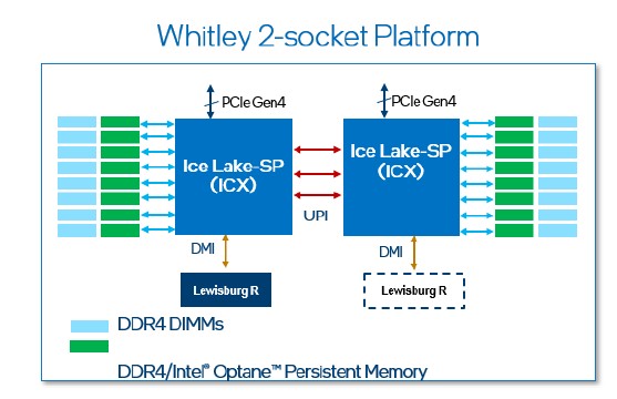
Just a reminder that the Ice Lake Xeon SPs require a new server platform, code-named “Whitley,” which is based on a modified “Lewisburg-R” C620A chipset, which is common across Skylake, Cascade Lake, and Cooper Lake servers. Here is a schematic of the Whitley platform:
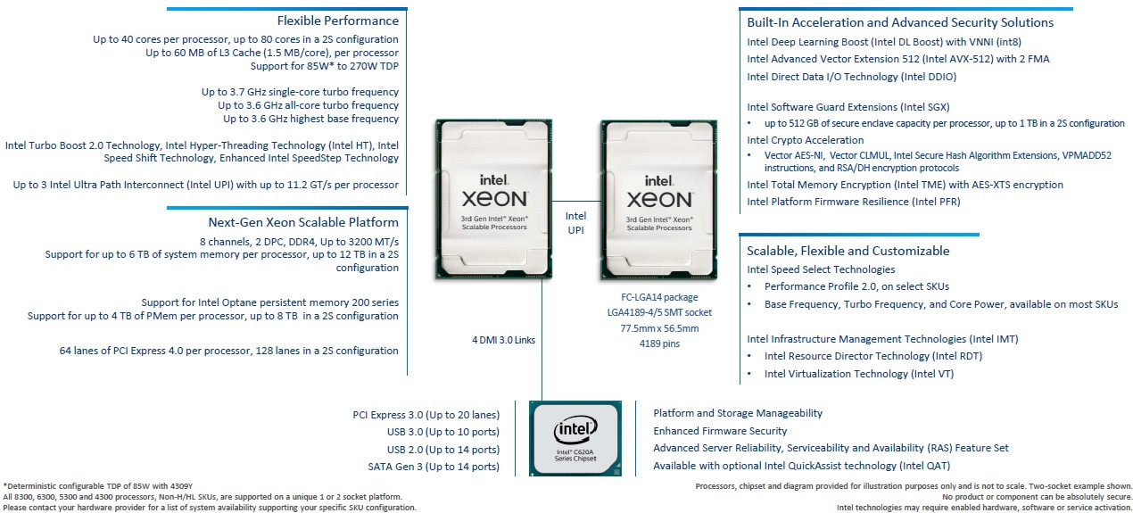
And here is a listing of some of the core features in this platform, most of which are expressed through the Ice Lake Xeon SP chip itself:
And here is a table that compares and contrasts the feature sets of the Cascade Lake and Ice Lake server CPUs in a nice compact form:
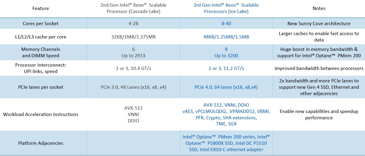
Here are the important things. First, Intel finally has eight DDR4 memory controllers on a single CPU socket and running at 3.2 GHz, which brings the Xeon SP family finally to parity with the rest of the server CPU industry. (That was a long wait.) This brings memory capacity up by 33 percent and memory bandwidth up by 33 percent; Intel has certified DDR4 DIMMs up to 256 GB in capacity each, and across eight controllers with two DIMMs per channel, that is 4 TB of memory per socket maximum. If you use a mix of DDR4 and Optane 3D XPoint memory in DIMM form factors, you can stretch the main memory capacity to 6 TB per socket.
The Ice Lake server CPU also has PCI-Express 4.0 controllers, which are necessary for a lot of networking, storage, and compute acceleration peripherals. The number of PCI lanes per socket has increased to 64, up from 48 lanes with the Cascade Lake processor; and the lanes run twice as fast, so the aggregate I/O bandwidth per socket has gone up by 2.7X moving from Cascade Lake to Ice Lake. This will allow a lot more peripherals to hang off the Ice Lake CPUs than was possible with the past two generations of Xeon SPs and even earlier Xeons.
Unlike AMD’s Epyc family, Intel has specialized UltraPath Interconnect (UPI) links to create NUMA coupling between processors, and the Ice Lake Xeon SPs have two or three UPI links per socket (depending on the model) to lash the processors together. The Ice Lake Xeon SP UPI links run at 11.2 GT/sec, which is 7.7 percent faster than the links in the Cascade Lake server chips.
What the use of UPI links means for Intel is that valuable PCI-Express lanes in a two-socket configuration are not used up when two processors are linked to each other. The AMD Epyc architecture has a superset of functions that ride atop PCI-Express links that turns them into what it calls Infinity Fabric, which can be thought of as a subset of the HyperTransport NUMA links used in the Opteron X86 server chips from days gone by. So, an Epyc Rome or Milan socket has 128 PCI-Express lanes running at PCI-Express 4.0 speeds, which is great and which is twice as much as the 64 lanes in the Ice Lake Xeon SP. But when you gang up two Rome or Milan chips, you lose 64 lanes out of each chip to create the NUMA links between the two processors, so you only end up with 128 lanes remaining out of the chips to go to peripherals like GPU accelerators. That’s the same lane count in a two-socket Ice Lake Xeon SP setup. That’s precisely enough to support eight x16 slots for accelerators and nothing more.
Aside from myriad changes to the microarchitecture, which we will get into separately, the big changes are that the cores how more cache to play with. L1 cache weighs in at 48 KB per core for the Sunny Cove cores, up 50 percent over the Cascade Lake cores; L2 caches are 1.25 MB per core, up 25 percent; and L3 caches are 9.1 percent bigger at 1.5 MB segments per core.
That leaves the actual Ice Lake SKUs. So, without any more ado, here they are:
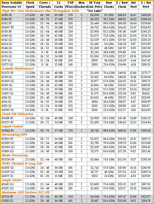
There seems to be a SKU for just about every season and reason. By our count, there are 36 truly unique models in the Ice Lake Xeon SP lineup, coming with the usual Platinum, Gold, and Silver designations that govern how much and how fast various features are on the chip. The Ice Lake chips marked in gray have the maximum capacity of 512 GB for SGX security enclaves, which we will describe separately. The price/performance of these chips is all over the map, and we will be drilling into it separately as well.

MGX: Nvidia Standardizes Multi-Generation Server Designs
Updated With More MGX Specs: Whenever a compute engine maker also does motherboards as well as system designs, those companies that make motherboards (there are dozens who do) and create system designs (the original design manufacturers and the original – get a little bit nervous as well as a bit …
Arm Gets Closer To Creating Full-Blown Server CPU Designs
It takes too long to get a new compute engine in the field, and everybody complains about it. Customers are impatient because they want more performance and the better bang for the buck that always comes with a new generation of chips. And those who make CPUs, GPUs, and other …
Drilling Down Into The SiPearl European Arm Server Chip
The European Union has made it clear that it wants to be able to stand on its own two feet in the design of server processors, for both general purpose uses and for exascale-class supercomputers. It is a difficult task, and one that Silicon Pearl, a French startup founded by …
No financial damage to Intel?
Come on, AMD has done a lot of that to snarky, bribing and cheating Intel that has milked us for too long.
Would never buy Intel!
None that affected its top line or bottom line by as much as Opteron did.
Thanks. Good article. Intel mentioned that the N versions of these Ice Lake Server chips are their selection for networking applications. Any idea what are the features in those chips that makes them preferred for networking?
One more question, since you mentioned Sapphire Rapids. There were some stories today, for example on tomshardware, providing some more leaked details on Sapphire Rapids. In particular, they listed up to 64GB of HBM2E per socket … which has an obvious benefit … but also the use of the Data Streaming Accelerator. This is the first I’ve seen of the DSA, but I found a surprising amount of info on it on-line, including a full spec. However, I hope you can examine this at some point and provide some insight about its potential use cases and relative advantages over the current implementations of dma or nvme.
Great article, one little oversight…
Cooper Lake processors have up to six UPI links per socket, double the number available on Ice Lake.
Yup. I just keep misremembering this.