

Without question, the biggest bottleneck in artificial intelligence and for a lot of HPC workloads today is bandwidth. Bandwidth at the network level; bandwidth at the socket level; bandwidth at the compute and memory level. No matter how many teraflops one single chip can push at high precision, once your workload scales beyond a single accelerator, node, or rack, bandwidth quickly becomes the limiting factor.
We have seen chipmakers grapple with this on a number of levels, by packing more high-bandwidth memory onto their chips, boosting interconnect speeds, and by using chiplets to push beyond reticle limits. Intel’s “Ponte Vecchio” Max Series GPU and AMD’s recently announced “Antares” Instinct MI300X GPU are prime examples of the latter. Driving data between chiplets does introduce I/O bottlenecks in its own right, but we can’t exactly make the dies any bigger.
Aside from needing a socket that is bigger than the reticle limit of lithography machines, we still need more capacity to satiate the demands of modern AI and HPC workloads. Over the past few years, we’ve seen a trend toward denser boxes, racks, and clusters. Cloud providers, hyperscalers, and GPU bit barns are now deploying clusters with tens of thousands of accelerators to keep up with demand for AI applications. It’s at this beach head that silicon photonics startup Lightmatter, now valued at more than $1 billion, believes it has the market cornered.
“Over the next few years, all of the GPUs in the world that are designed for AI training and inference or high-performance computing are going to be built on Passage,” Lightmatter chief executive officer Nick Harris boasted in an interview with The Next Platform.
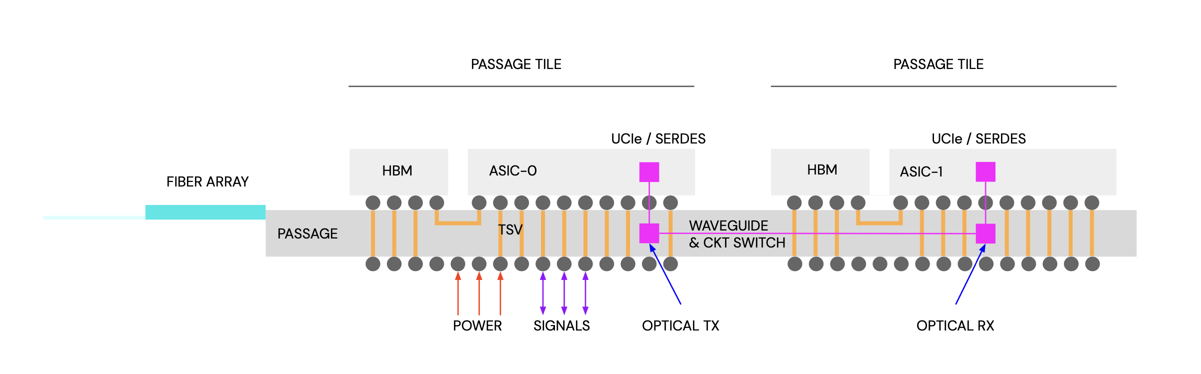
Lightmatter’s Passage is a silicon photonics interposer designed to support high speed chip-to-chip and node-to-node communications. Silicon compute and memory dies can be attached to the surface of Passage, while communication between the dies is handled either electrically or optically depending on the distance from each other.
To be clear, Passage isn’t trying to replace all of the chip-to-chip interconnects, like those found all over Intel’s Ponte Vecchio or AMD’s Antares GPUs, with optical ones.
“Let’s say you have HBM on a Passage tile, the link between the HBM and your processor is electrical. It’s when you scale out those links that are inch scale, those are optical,” Harris explained. Like an optical HGX:
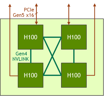
Lightmatter isn’t naming customers just yet, but looking at modern compute platforms from Intel, AMD, and Nvidia it’s not hard to see where Passage might fit. Your typical GPU node is built around a carrier board which usually interlinks four or eight accelerators in an all-to-all configuration so they can work together as a single unit of compute.
However, compared to what is possible using die-to-die interconnects, socket-to-socket communication can be an order of magnitude slower. “You’ve got the die-to-die millimeter interconnects that have a certain bandwidth, and then when you go to the PCB level, it drops by a factor of 10X,” Harris says.
Looking at Nvidia’s HGX boards, the chipmaker is able to achieve around 900 GB/sec of bandwidth, which works out to 7.2 Tb/sec, between each of its accelerators using NVLink. By comparison, Harris claims Lightmatter has a project coming out that’s 60 Tb/sec leaving the chip, which is 7.5 TB/sec of bandwidth per chip.
The break out below, shows how eight compute dies could be meshed together using Passage, but it’s not limited to that. Lightmatter says it can fit up to 48 reticle-limited dies onto a single package if you wanted to.
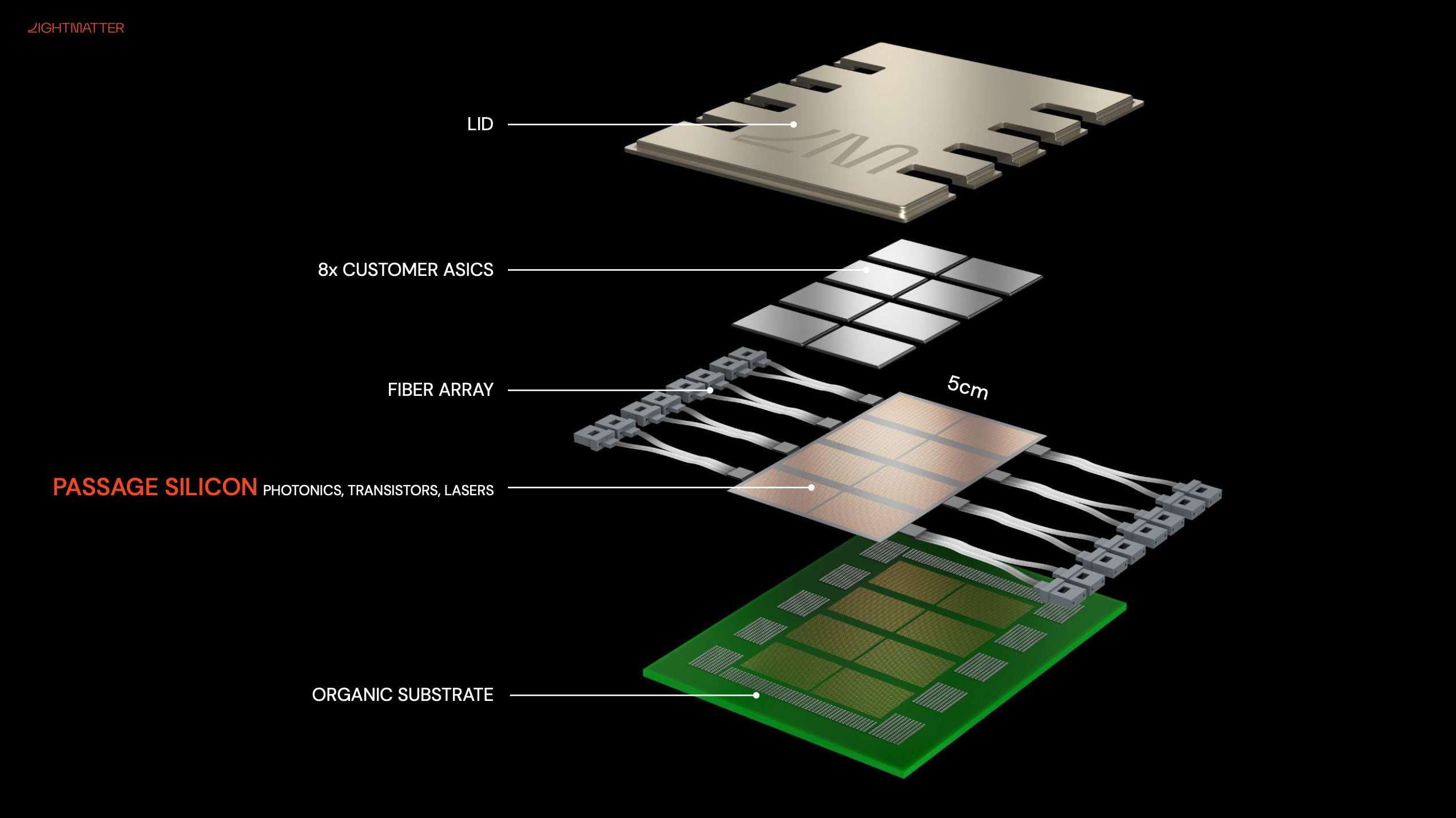
The connection between the silicon and Passage is electrical and the opto-electrical conversion happens within the interposer itself. This means Passage can be remapped to accommodate new chips while also eliminating the need to integrate photonics into the compute itself.
“What we do is we change the floor plan of Passage so that we can map where their I/O pins and where their power pins are to deliver power through the TSVs,” Harris says. “Then the I/O pins will either hit an optical modulator to send data inside Passage or off Passage, or they’ll pass through and go to the host CPU on the board. We make Passage look like a purely electrical interposer.”
Scaling To The Rack And Beyond
As we alluded to earlier, training large AI models on a reasonable time table requires accelerators. Nvidia achieves this using its NVLink switch appliances to mesh up racks worth of GPUs while its InfiniBand or Spectrum-4 Ethernet switches keep the systems fed with data.
According to Harris, this kind of switching is largely unnecessary thanks to fiber attach points integrated into the edge of each Passage tile. As we learned at Hot Chips in 2022, each of these attach points provides up to 16 TB/sec of bandwidth, which can be used to interconnect multiple tiles together.
We have seen a similar approach employed by Intel’s Habana Gaudi2 accelerators which feature two dozen 100 Gb/sec Ethernet ports – 21 for the all-to-all mesh and three for node-to node communications – which eliminate the need for additional NICs.
The difference here is Passage also supports optical circuit switching functionality, which can be programmed on the fly. According to Harris, this has a couple of benefits, particularly for AI training workloads.
“When you compile an AI training program, you know the execution deterministically. It doesn’t change dynamically while the program is running. So you can know what the entire wiring diagram needs to be like ahead of time. And that means you can program a topology out of a huge number of computers,” he says, claiming Lightmatter now has customers using Passage to “scale to 300,000 node supercomputers.”
Who these customers are, Harris wouldn’t divulge, but he did say the company was working with major semiconductor partners and cloud providers which were “buying in massive volumes.”
Harris adds that these large clusters aren’t fixed and can be partitioned out to address changing customer demands. “So maybe a 4,096 node cluster can be rented out as 256 nodes. It lets you slide and dice this huge investment,” he said.
Silicon Photonics In The Spotlight
Silicon photonics vendors have come into the spotlight over the past few years as a ramp in AI interest drives demand and – more importantly for the startups themselves – investment in faster interconnect technologies.
“AI – what an ally for high performance computing,” Harris says. “People are just spending unlimited money. Blank checkbook, spend whatever you need to win the AI race, and that’s a great environment for a technology like photonics and Passage.”
In December, Lightmatter pulled in $155 million in a second Series C funding round, bringing its total funding to $420 million and pushing the company into unicorn territory.
With that said, Lightmatter is hardly the only silicon photonics startup riding the AI hype train. Earlier this year, we looked at another startup called Celestial AI, which had raised $100 million for a silicon-photonics interconnect of their own. Much like Lightmatter’s Passage, Celestial’s Photonic Mesh spans chip-to-chip, package-to-package, and node-to-node connectivity.
Then, of course, there’s Ayar Labs, which has been developing silicon photonics chiplets going back to 2015. The chipmaker’s TeraPHY first cropped up in 2019 and is designed to provide optical I/O for data going on and off the package. In September, we looked at an embarrassingly parallel graph processing unit developed by Intel under contract for DARPA that used Ayar Labs to scale to millions of threads. To date, the company has raised about $220 million, including a $130 million cash infusion from Intel and Nvidia in early 2022.
Separately, back in 2022, Nvidia offered a peek at what a future optically linked GPU system might look like.
Suffice to say there’s no shortage of competition in the silicon photonics space these days. And the market is going to need it because we are going to need several ways to skin this bandwidth cat.


This is nothing spectacular. You should investigate APIC Corporation in Culver City CA.
Celestial’s 7.2 Tb/sec per mm² was quite impressive (and so was Ayar Lab’s approach to material selection in CPO, and Google’s reconfigurable optical interconnect for TPUs) but the nice diagrams provided here for Lightmatter’s Passage really sell the tech very well for me. I love that it’s an interposer, as that is truly integrated into the chip, under the chiplets, with structural stability. Having 48 reticle-limited dies per package should work nicely in a variety of situations. But, especially, 60 Tb/sec per chip, across packages, is fantastic (to me).
This should really help make disaggregated composable systems a properly performing reality (eg. with CXL 3+) I think.