
At some point, Moore’s Law increases in performance are going to hit a wall when it comes to datacenter networks. But we are not there yet, and the research and development work is progressing so that just about the time switch and router ASICs hit a wall, we should have silicon photonics to help increase the density and power efficiency of network devices so we can continue to build out the network.
Intel has, of course, been working on silicon photonics for a long time, and the people within its Connectivity Group, which is headed up by Craig Barratt, formerly chief executive officer at Barefoot Networks (which Intel acquired last June to build out its Ethernet switching business), have been showing off some of the technologies that are either just being commercialized now or are set to soon be coming to market as they relate to co-packaged optics and silicon photonics. To be specific, Hong Hou, general manager of the Silicon Photonics Products Division (SPPD) within Connectivity Group, and Ed Doe, general manager of the Barefoot Networks Division, walked us through some of the advances that Intel and Barefoot have been working on.
Global data traffic from datacenters to users – the so-called “north south” traffic – has been a tiny slice of the bits pumped through the networks of the world for a long time. The traffic between datacenters (which doesn’t have a name, but you might call it “northwest by southeast” if you wanted to be clever) has also been a relatively small portion of the datacenter traffic pie for a long time, too. But as applications have become more distributed and interdependent (not just because of containers, but certainly exacerbated by them), the bandwidth requirements and radix of the networks inside of datacenters has been exploding. Like this:
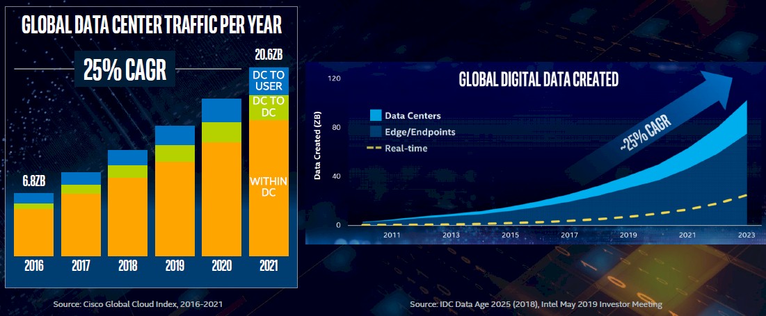
Not only is there a 25 percent compound annual growth rate for this traffic in and around the datacenter, growing from an aggregate of 6.8 ZB in 2016 in a pretty linear fashion to 20.6 ZB by 2021 – those are zettabytes, which are 1,000 exabytes each. The ratio of annual traffic inside the datacenter compared to global internet traffic was 6:1 in 2019, and that datacenter traffic was an incredible 11.6 ZB.
The amount of data created and stored, as the chart on the right above shows, is also rising at a 25 percent CAGR, and is considerably larger than the amount of data transmitted over datacenter networks. The datacenter will be a small part of all of this created data, and much of it will either be processed in real-time and never stored or created at the edge and either stored there or not as conditions dictate. Both of these curves are slightly exponential, and the amount created is a bit more exponential based on our eye.
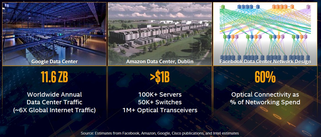
This data growth is causing all kinds of issues in the datacenter. Take a typical hyperscale datacenter as an example. In this case, Hou tells The Next Platform, it has over 100,000 servers and over 50,000 switches – and that is probably a lot more switches than many thought were needed to build the massive Clos architectures that hyperscalers employ. But the interesting bit, at least as far as Hou is concerned since he runs the silicon photonics business at Intel, is that one of these hyperscale data centers needs to have over 1 million optical transceivers, which are not cheap and which contribute mightily to the overall cost of the datacenter infrastructure. To put a number on this, the optical transceivers at the end of the fiber wires that link nodes to switches and switches to each other represent somewhere between $150 million to $250 million in spending for a hyperscale datacenter, and that spending is usually depreciated over five years like the rest of the server, storage, and switching gear. Add up all of the regions for the hyperscalers and cloud builders, and then all of the datacenters they operate, and this really starts adding up to several billions of dollars a year in spending just on optical transceivers each year. By the way, those optical transceivers represent about 60 percent of the overall network budget at these datacenters – more than switches, more than NICs, and more than cables and more than all of them added together, at least as far as the data that Intel has gathered is concerned.
Hou admits there is some wiggle in these figures, depending on the company, but clearly as bandwidth needs grow and actually require optical transceivers, there is growing demand. But there is a problem.
“These optical transceivers all need to be made with a consistency and scalability within a matter of a couple of months in order to enable the cloud service providers to commission a datacenter, put it into service, and generate revenue,” explains Hou. “The traditional boutique optics using discrete components, which does not give you that rapid rate of manufacturing scalability. Also, in order to service this level of customer demand, capital expenditures might be too heavy for traditional optical suppliers.”
This is the same argument that Intel has been making for more than five years as it tried to drive HPC system sales through its partners with a more consistent, off-the-shelf hardware and software stack, and why it eventually became a prime contractor on the “Aurora” pre-exascale supercomputer (which was canceled for reasons Intel and Argonne have never really explained) and the 1.3 exaflops “Aurora A21” system that it was transformed into. Cray is the system manufacturing partner on this Argonne system, and had Hewlett Packard Enterprise already have acquired Cray two years ago, HPE would be the prime contractor for this machine as it is for the other two exascale systems being built by the US Department of Energy – the “Frontier” system at Oak Ridge National Laboratory and the “El Capitan” system at Lawrence Livermore National Laboratory. Intel is best when it is a reliable component supplier, and in our opinion, it never should have been a prime contractor for systems itself; it makes plenty of money without having to take business away from its partners.
We suspect that Intel’s long-term vision might be to provide end-to-end networking – switches, NICs, optical transceivers, and cables – to hyperscaler, cloud builder, large enterprise, and telco and service provider customers, particularly if it is investing so heavily in all of the components. A lot depends on what the rest of the ASIC and switch and NIC makers do.
The question we have it what percentage of that more than $1 billion it takes to build a hyperscale datacenter is going to networking. We have heard that at its peak, the networking component of one of these datacenters was 10 percent and approaching 15 percent, but apparently it is back down again.
“It tends to oscillate, but it has never been below high single digits,” explains Doe. “It obviously depends on how some of those datacenters are being built. I think both Hong and I are exposed a little bit to those customers that actually use a large number of switches and optical transceivers, but not everybody builds their network the same way. Some build it with higher levels of oversubscription, and as a result, they need fewer switches and fewer optical transceivers. Some of them use up to nine layers of switches, which is how you get to that ratio of two servers for every switch and 20 to 30 optical transceivers per switch gets to that math. In this case, it would definitely be up towards the 15 percent and potentially even higher cost of the overall datacenter. But in other in other cases where they do four layers of switches and have more oversubscription, you are going to immediately cut the number switches down and therefore the number of optical links as well. But that is why bringing these technologies in the optical transceivers together is so important because it is such a dominant part of the overall network cost.
Intel started its silicon photonics research more than two decades ago to reach this moment put its first silicon photonics optical transceivers into the field in 2016 and has been quietly ramping up production in that time. By the end of 2018, it had shipped its first 1 million units, and through the end of 2019, it had sold 3 million units and was set to add another 500,000 units in Q1 2020 alone, keeping that 2 million a year pace going. Here are the two different silicon photonics optical transceivers that Intel has in production:
![]()
The first one, the 100G PSM4 QSFP, has a 2 kilometer reach on a parallel single mode fiber and has an indium phosphide layer on the transmitter chip that implements four hybrid lasers and modulators for converting electrical signals to light and photodetectors to convert the light back into electrical signals in the detector chip in the package. This device obviously supports 100 Gb/sec speeds. The more recent 100G CWDM4 QSFP optical transceiver uses duplex single mode fibers and uses carrier wave division multiplexing to take the output from the same laser/modulator circuits and pump 100 Gb/sec of bandwidth over that single fiber. It has a 10 kilometer maximum reach, with options for 500 meters and 2 kilometers.
The on-chip lasers in the latter transceiver is rated at between -40 degrees and 85 degrees Celsius, which means it can be used in a wide range of outdoor environments where equipment is kept dry but not necessarily at the same temperature as a modern datacenter. More importantly, says Hou, the defect rate of these new transceivers is on the order of 28 per million compared to around 1,000 per million with the industry standard optical transceivers available from other suppliers. Hyperscalers, cloud builders, and telcos, and service providers do not like to repair or replace equipment, so this resonates, and that is why, says Hou, Intel has the number one market share in 100 Gb/sec optical transceivers for single mode fiber.
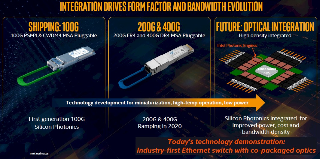
As you can see from the roadmap above, Intel is currently working on its 200G FR4 and 400G DR4 optical transceivers, which as the names suggest, will support ports running at 200 Gb/sec and 400 Gb/sec. These will be launched and ramped this year.
But ultimately, what you really want to do is have silicon photonics ports right on the switch ASIC package, consolidating the transceivers on the switch end and, although Intel didn’t talk about this, you could do the same thing on the server NIC end too with a SmartNIC design that had some hefty CPUs or FPGAs on it.
About eight months ago, in the wake of the Barefoot Networks acquisition, the switch and silicon photonics people in the Connectivity Group set out to do just that, testing the idea out on a switch using the “Tofino 2” switch ASIC, which is a chiplet design that sports 12.8 Tb/sec of aggregate bandwidth. Here is that Tofino 2 chip surrounded by co-packaged 100 Gb/sec optical tiles:
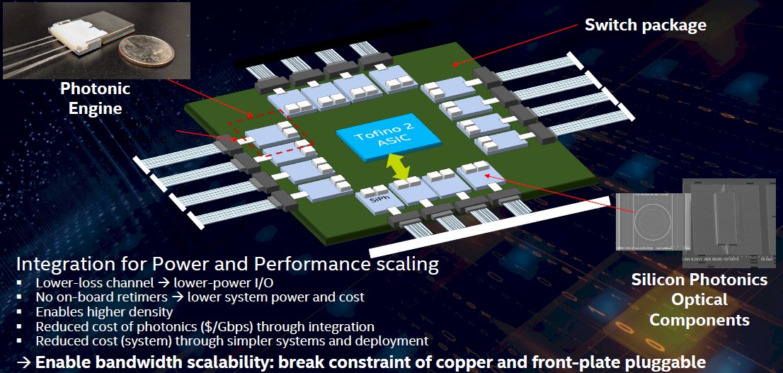
This particular Tofino 2 switch was set up to drive 400 Gb/sec ports, and importantly, this integration will shave about 30 percent off the overall networking costs and 30 percent off the power just because of the integration of the transceiver circuits on the switch ASIC package.
This is considerably better than can be done with optical switches that have external lasers in the switch chassis (which are in tern better than optical modules in the front panels of switches that have retimers hooking them into switch ASICs.) The co-packaged optics yield the best density and power reduction, too. With that power reduction, now the SerDes on the switch ASICs can be ramped faster and then get everything into a two-year cadence of doubling. That’s the idea, anyway.
The photonics engines that Intel is demonstrating are running at 1.6 Tb/sec today (that’s 16 channels at 100 Gb/sec with PAM4 encoding), but are scalable to 3.2 Tb/sec per tile and that means that can front-end future Tofino chips that have 25.6 Tb/sec, 51.2 Tb/sec, and even 102.4 Tb/sec of aggregate switching bandwidth. The Tofino 2 chip doesn’t have the 100 Gb/sec SerDes, but the follow-on Tofino NG chip coming perhaps later this year and its two follow-ons will, which will probably have one last speed bump to faster SerDes (100 GHz with PAM4 encoding seems likely) before switch circuits hit their Moore’s Law limits. Integrating the optics with silicon photonics is going to be key, and probably with 100 GHz SerDes speeds for sure, and maybe with later generations of 50 GHz, which is where we are at today.
Given all of this, saving power and money on optics will mean allowing switch ASICs to burn a little hotter and to get a little larger, which they will have to do somewhere around the 5 nanometer or 3 nanometer generations. This way, the overall thermals and costs of the switch/transceiver complex will still go down in cost and thermals, and that is a kind of keeping Moore’s Law alive, as Intel would argue.

How Lightmatter Breaks Bandwidth Bottlenecks With Silicon Photonics
Without question, the biggest bottleneck in artificial intelligence and for a lot of HPC workloads today is bandwidth. Bandwidth at the network level; bandwidth at the socket level; bandwidth at the compute and memory level. No matter how many teraflops one single chip can push at high precision, once your …

Building An Ecosystem for Heterogeneous Memory Supercomputing
The drive toward exascale computing is giving researchers the largest HPC systems ever built, yet key bottlenecks persist: More memory to accommodate larger datasets, persistent memory for storing data on the memory bus instead of drives, and the lowest power consumption possible. One of the biggest challenges architects and operators …
Luminous Shines A Light On Optical Architecture For Future AI Supercomputer
It is not every day when we hear about a new supercomputer maker with a new architecture, but it is looking like Luminous Computing, a silicon photonics startup that has been pretty secretive about what it was up to, is going to be throwing its homegrown architecture into the ring. …
Great article! Any thoughts on the Nvidia buyout of Mellanox with respect to these 100G + densities?
Dear Mr. Morgan,
You are making surprising claims in this article. For example, you claim that a “hyperscale” data center will have:
≥ 1EE6 optical transceivers
≥ 1EE5servers
≥ 5EE4 optical switches
That would mean:
(# transceivers)/(# servers) = 1EE6/1EE5 = 10 ??
(# switches)/(# servers) = 5EE4)/1EE5 = 0.5??
So few transceivers and switches?
Well, I am not making any claims. But Intel is. The total number of transceivers has to exceed the number of servers, and it depends on the topology and tiering in the network. The number of switches will be fewer than the number of servers, but maybe only by half as Intel has suggested.