

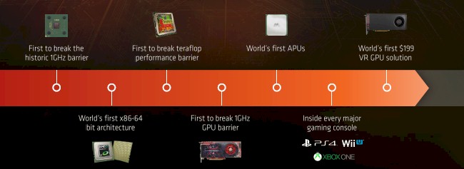
It is funny to think that Advanced Micro Devices has been around almost as long as the IBM System/360 mainframe and that it has been around since the United States landed people on the moon. The company has gone through many gut-wrenching transformations, adapting to changing markets. Like IBM and Apple, just to name two, AMD has had its share of disappointments and near-death experiences, but unlike Sun Microsystems, Silicon Graphics, Sequent Computer, Data General, Tandem Computer, and Digital Equipment, it has managed to stay independent and live to fight another day.
AMD wants a second chance in the datacenter, and as we talked about back in March, it has been working hard for the past five years to re-engineer itself and re-architect its CPUs and GPUs so they can get back into the datacenter game. AMD has been a processor and server innovator in the past, and it intends to be one again, and the future “Naples” Epyc multicore X86 processors and “Vega” GPU coprocessors are the first step in a multi-year journey back to the glass house for AMD.
For now, we are going to just zero in on the Epyc X86 server chips, but bear with us, we will come back around to heterogeneous computing in a follow-on article.
Past Is Prologue
Past performance is not an indication of future performance, and no one knows this better than Wall Street. But the central theme at the Financial Analysts Day event with Wall Street that AMD hosted this week was a history lesson that showed how AMD was on the cutting edge before and made money, and that it could get back there again and make money.
We do not think that AMD is going to have another Opteron moment like it did back in 2003 with the “Hammer” line of processors, where a stubborn Intel was defending its 64-bit Itanium and only gradually increasing the core counts on its 32-bit and memory constrained Xeon processors. The Opterons had HyperTransport interconnect that blew away the Front-Side Bus architecture of the Intel chips, a sophisticated caching hierarchy, integrated memory controllers, and a multicore architecture from the get-go. AMD caught Intel with its technical pants down, and it scared Intel so badly that by 2009 the Itanium was basically dead and the “Nehalem” Xeons launched by Intel into the maw of the Great Recession cloned a lot of the technologies invented by AMD with the Opterons.
This seems only fair, since AMD rose to prominence by cloning and then extending Intel’s CPU work. And while AMD makes much of the fact that it is an innovator in GPUs as well as CPUs, we all have to remember that this is not homegrown technology, but rather the result of the its acquisition of GPU maker ATI Technologies in July 2006 for $5.4 billion. ATI, you will remember, also made chipsets for the Opteron server line, which is another reason why AMD was interested in acquiring it. Given all of the talent embodied in ATI, which was the archrival of Nvidia, the combination of the two companies was logical and natural, and the multi-pronged attack that AMD is undertaking back to the datacenter will deploy all of its CPU and GPU smarts. The competitive opportunity is not as large as it was back in the early 2000s when the Hammers entered the field, but AMD believes it can – and will compete it get back its rightful share of the X86 server racket.
The One Socket Upper Cut
Having said all that, Intel is kind of all over the map with processing, with Xeon E3 and Xeon D at the low end, a converging Xeon E5 and Xeon E7 at the middle and high-end, and the Xeon Phi for massively parallel work that might otherwise end up on a GPU. There is also the “Kittson” Itanium that Hewlett Packard Enterprise will start shipping imminently in its high-end Integrity Superdome systems, which we will cover later this week, and Altera FPGAs and Nervana machine learning chips. And there is, as AMD’s top brass suggested to Wall Street, an opportunity to shake up the stodgy two-socket servers that dominate the datacenters of the world and downshift a lot of them to very fast single-socket boxes. Intel is simplifying its life greatly by melding its Xeon E5 and Xeon E7 families into a unified line that spans from two to eight sockets using the “Skylake” Xeon processors.
Way back in the day with the Opterons, AMD had different SKUs and chipsets and sockets for machines with one, two, or four sockets, just like Intel has done, and it also had low voltage and therefore low wattage parts to try to carve out a niche with the hyperscalers – which it did, even though no one would talk about it publicly. (We have seen the Google motherboards with Opteron sockets on them, and similar ones from Dell’s custom server division, too.) But this time around, AMD is going to compete with Intel in the core server market by offering no holds barred systems with all of the tops of the features ripped off and running at peak speeds in both single-socket and dual-socket configurations. AMD is not at all interested in going after the four-socket server market, and here is why:
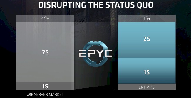
It is not so much that AMD is going to make a play for the one-socket server space as it is that AMD is going to convince mainstream customers using two-socket Xeon servers with modest core counts and prices that they can get the same performance and memory and I/O bandwidth from a single-core Epyc system as they can get from a two-socket Xeon machine with modest core counts and some caps on features. And while AMD did not make comparisons to the current “Kaby Lake” Xeon E3-1200 v6 processors, we presume that it will be able to take these on, too, and also give the Xeon D, which is stuck at the “Broadwell” generation at the moment, a run for the money, too, among hyperscalers like Facebook that deploy it.
At the moment, about 80 percent of the server units shipped, based on 2016 data from IDC, have two sockets, with 9 percent being represented by machines with four sockets or more and another 9 percent coming from single socket machines. There are not a lot of single-socket machines in enterprise and hyperscale datacenters because of the memory capacity and memory and I/O bandwidth limitations on the processors that are typically used there. Machines with two sockets have twice as much of all this stuff, even if you don’t need all of those cores. That is why AMD is targeting the mainstream Xeon E5 servers with its single-socket Epyc machines and the top-bin Xeon E5 machines and low-end Xeon E7 machines with its two-socket Epyc machines. And by doing so, it thinks it can disrupt the status quo in the datacenter.
The last battle was about 64-bit memory addressing and multicore processing. This one is about form factor, performance, and total cost of ownership, particularly when you consider that a lot of enterprise software is priced based on the socket count, not the number of cores. Here is how Forrest Norrod, senior vice president and general manager of the Enterprise, Embedded, and Semi-Custom group at AMD and the guy who started Dell’s Data Center Solutions custom server business (which used to be the go-to for Facebook before it launched the Open Compute Project), cased the situation in the two-socket space:
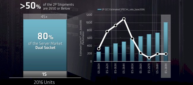
This is a very interesting chart indeed, showing the relative integer performance and shipment volumes of the Broadwell Xeon E5 v4 processors. As you can see, more than half of the volumes are for mainstream parts, not the top bin, 24-core part that is, as we discussed when they were launched last spring, very pricey indeed.
Back in March, as the Ryzen desktop chips based on the Zen cores were being launched, Norrod trotted out some benchmarks pitting the future Naples Epyc chips against the current Broadwell Xeons running a seismic reservoir simulation that was very much memory bandwidth bound, and it showed that the top-bin Epyc part with two 32-core processors and 512 GB of memory could best a Xeon E5 that is, by comparison, constrained on memory and I/O bandwidth by a factor of 2.5X on this benchmark. Some people complained that this seismic benchmark did not stress the cores in the same way and that it was showing off the memory bandwidth of the Epyc platform, which drove 170.7 GB/sec compared to 76.8 GB/sec for a two-socket Xeon E5-2699A v4 processor.
This time around, to quell some of the criticism from that first benchmark test, AMD is looking at a job that is very CPU intensive and does not stress the memory quite so much. Norrod chose the compilation of the Linux kernel, based on Ubuntu Server, as the test. Two sets of benchmarks were run, one pitting a single-socket Epyc system against a mainstream two-socket Broadwell Xeon E5 machine and another pitting a two-socket Epyc against the top bin two-socket Xeon E5 system.
Here were the configurations for the one-socket Epyc versus the mainstream Xeon two-socket:
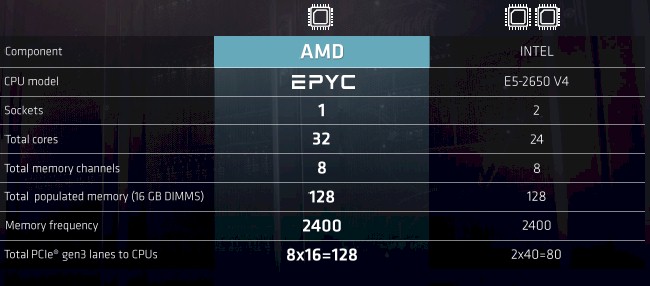
On the Linux kernel benchmark test, it took the 32-core Epyc system 33.7 seconds to do the compile, and the two-socket Xeon E5-2640 v4 system did it in 37.2 seconds. Advantage to the Xeon was only 1.5 percent, which is not much of a difference when you consider how much more stuff goes into that two-socket Xeon box. Take a look at the scale of the infrastructure of the Xeon and Epyc motherboards used in this test:
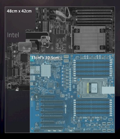
This is not precisely a fair comparison because the Intel motherboard is T-shaped, not a square. Some of that area is used for power supplies and peripheral adapters.
“The Epyc is a much denser solution, and it uses a lot less space and a lot less power, but still provides more cores and more I/O with slightly better memory bandwidth than that mainstream Intel system,” Norrod explained in his presentation. “So for us, we have got the opportunity to really disrupt the volume two-socket market. Our one socket strategy is not about doing a better one socket. Our one socket strategy is about offering customers a highly optimized, enterprise or cloud capable single socket alternative to the two-socket systems that hitherto they have been forced to adopt if they wanted a certain amount of memory performance or I/O capability.”
Norrod added that the single-socket Epyc system would offer about a 30 percent TCO advantage over the mainstream two-socket Xeon server, and we think that 20 percent is the threshold for any hyperscalers, HPC centers, or enterprises to think about switching.
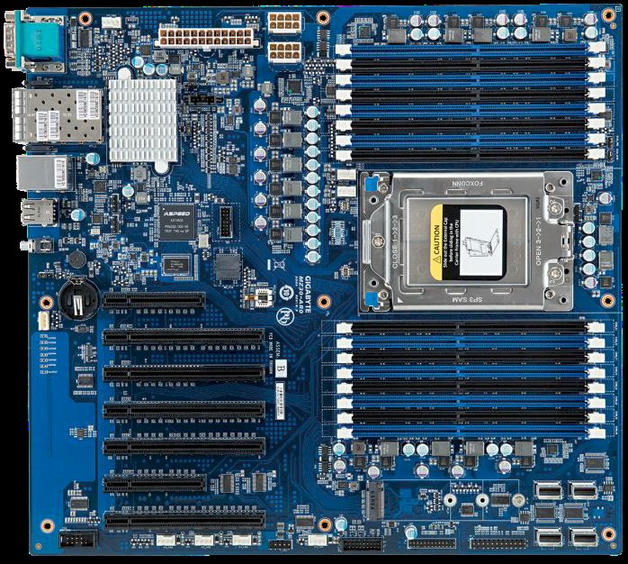
For fun, here is a zoom shot on that Epyc motherboard:
What Norrod says is backed up by what we can see in the motherboards tested and what we know about the impending Skylake Xeons. The single-socket Epyc machine is obviously a lot smaller, and if you do the math, it is a little less than half the area for essentially the same performance, with the same memory footprint and slightly better memory bandwidth and 60 percent more I/O bandwidth.
Form factor is perhaps not sexy to everyone, but these are great numbers.
Intel can do a single-socket Xeon E5 part with the Skylake generation, but as far as we know, there are only going to be 48 lanes of PCI-Express 3.0 traffic for I/O and it will only have twelve memory slots across six memory controllers, compared to the 128 PCI-Express 3.0 lanes, eight memory channels and sixteen memory slots for the single-socket Epyc.
The two-socket Epyc is no slouch, either. Here are the two configurations that Norrod pitted against each other on the Linux kernel compilation test:
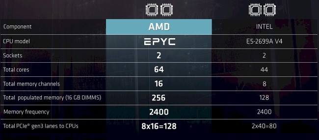
Those extra memory channels mean the Epyc machine can have twice the memory capacity if you keep the capacity of the memory sticks constant. This doesn’t seem particularly apples to apples, to be fair. But the Xeon would have to use memory sticks that are twice as dense, and more than twice as expensive, to match capacity. The Epyc setup has 64 cores, which is 45 percent more than the Xeon E5 setup and this will cut against AMD for software stacks that have per core, rather than per socket, pricing. It plays into AMD’s favor for software that is priced per socket, particularly when you look at the performance. On the Linux kernel compilation test, it took the two-socket Epyc machine 15.7 seconds to do the compile, compared to 22.5 seconds on the Xeon E5 machine using the top-bin part. That is 30 percent better performance for the AMD system, and it also implies that on this kind of work, the Broadwell core does about 11.7 percent more work than a Zen core at their respective clock speeds. We expect for the Skylake Xeon cores to have somewhere between 8 percent and 10 percent better instructions per clock compared to the Broadwell cores. If Intel gooses Skylake to 28 cores, the IPC goes up by 10 percent, but the clock speed goes down by 5 percent, then a two-socket Xeon should be able to do the Linux compile in about 18.5 seconds, we reckon. AMD will still have a 15 percent advantage on performance on this compute intensive job.
Epyc Better Not Fail
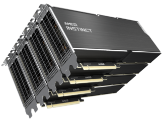
As we suspected back in March, the Naples processor is really a four-die multichip module, or MCM, that crams four eight-core chips onto a single package, all linked by the Infinity Fabric interconnect that has replaced HyperTransport and that we detailed here.
By shifting to an MCM – a trick that IBM, Intel, Hewlett Enterprise, and AMD have all used before in various processor generations – AMD can significantly cut the costs of producing a chip.
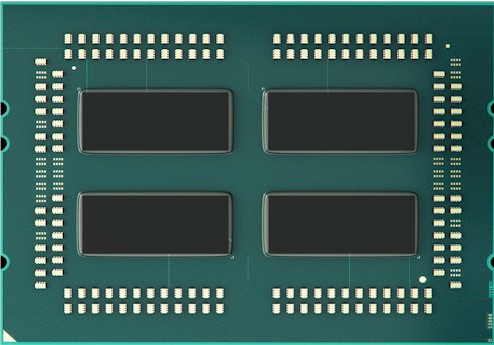
The reason this is true is because the bigger the chip is, the lower the yield there is on manufacturing it and the higher the cost of production for a good chip.
The trick is to have an interconnect that makes two or four of these dies look like a single die, and the wonder is why more vendors do not do this. But there are reasons why.
Instead of doing MCM trick, Intel makes one Xeon E3 die, one Xeon D die, three different Xeon E5 dies, and a Xeon E7 die, each with a different layout, performance level, and cost profile. The same Infinity interconnect that is used to link multiple sockets to each other is used to link multiple dies to each other inside the package and also to link out to PCI-Express peripherals and to main memory. AMD has not said how many Infinity Fabric ports are used inside the Epyc package, but it really is kind of like a baby NUMA cluster inside the package with each node having eight cores and two memory controllers each and 32 PCI-Express lanes exposed externally. It takes 64 Infinity fabric lanes to cross-couple two of these Epyc packages together, and we would not be surprised if there were lots of lanes linking these chips inside of the sockets.
To a certain way of looking at it, the Epyc chip is a four node NUMA cluster that is in turn clustered up to be an eight-node system. This is the upper limit of the NUMA scaling of the ATI server chipsets for Opterons, and that is no coincidence people. (The prior Opteron 6000 series were two-die MCMs, and the scalability of the ATI chipsets was maxxed out at four sockets, again topping out at an effective eight node NUMA.) This is the reason why AMD is really not doing four-socket Epyc machines. It used up the NUMA scaling inside of the package to reduce the cost of chip production so it can compete with Intel on price as well as on technology.
This is a smart tradeoff, but it does mean AMD has sacrificed the very profitable 9 percent of the market that is buying machines with four or eight Xeon, Power, Sparc sockets. Intel has Xeon dies with large core counts and integrated NUMA scalability precisely because it needs to offer this to compete against the big RISC vendors and also scale up the core count and the memory beyond two or four sockets. You can’t get to eight sockets with aggressive die splicing like AMD is doing, unless you have a very expensive external NUMA chipset, which adds latency and cost.
System architects have a heck of a time trying to figure out what Intel processor to use for a job, given all of the families and SKUs available. AMD will be keeping it relatively simple with the Epyc line, we think, with variants with one, two, or four dies in the package, for eight, sixteen, or 32 cores on the package. The memory and I/O bandwidth will of necessity scale precisely with the number of dies on the module, since these are hard cast. AMD will make a virtue out of this, of course. But it will have a fairly simple story to tell to the system architects, and that is good.
Perhaps more than anything, Epyc puts AMD back into the conversation, and because it is an X86 chip, it is the natural alternative to the Intel Xeon and will absolutely put competitive pressure on Intel. For all we know, Intel has been re-architecting Skylake in the past year to blunt the Eqyq assault on the core workhorse server space.
Lisa Su, chief executive officer at AMD, told Wall Street that with the Epyc CPUs and Radeon Instinct GPUs, the company was now chasing a $21 billion total addressable market, with about $5 billion of that being for GPU acceleration of HPC and machine learning workloads and the remaining $16 billion being for core compute inside of servers, storage, and switches. The Zen architecture and the resulting Epyc systems were created with the new datacenter in mind, Su explained, when AMD started its turnaround five years ago. With the GPU portion of the market growing at a compound annual growth rate of more than 75 percent between 2016 and 2020, AMD wants to get a piece of this action as well as taking a 5 percent to 10 percent slice out of the X86 server pie. (That data was not disclosed this week at the Financial Analysts Day, but comes from our prior conversations with Norrod.) AMD has not forgotten about its decade-long research and development into hybrid CPU-GPU architectures.
“The idea is to start thinking about the system before you start designing the silicon,” Su explained. “When we do that, and you look at workloads like machine learning or high performance computing, we can actually deliver breakthrough performance. And some of the ways we do this is by thinking about the flexibility that the workloads need upfront. One of the things that is unique about the I/O that we have chosen for Epyc is that it allows you to connect more GPUs directly to the CPU than any other solution in the industry.”
And that will set us up for the next story, which will be about how systems deploying the combination of Epyc processors and Radeon Instinct coprocessors to take on HPC, machine learning, and database acceleration workloads. And after that, we will talk about CPU and GPU roadmaps.

Now Comes The Hard Part, AMD: Software
From the moment the first rumors surfaced that AMD was thinking about acquiring FPGA maker Xilinx, we thought this deal was as much about software as it was about hardware. We like that strange quantum state between hardware and software where the programmable gates in FPGAs, but that was not …
With ROCm Software And Instinct MI200 GPUs, AMD Has Ecosystem Critical Mass
Paid Feature Great hardware is the foundation of any compute platform. But hardware, in and of itself, is never sufficient to create a platform. And in fact, it takes two other important things for any platform to be realized. After the hardware, a platform requires a complete stack of software …
Datacenter Will Be AMD’s Largest – And Most Profitable – Business
Two and a half years into the global coronavirus pandemic we all have upgraded our home IT infrastructure. And after several fibrillatory interest rate shocks by the major governments to try to curb inflation in the world economy, spending on PCs has consequently taken a nose dive. And a glut …
“get the same performance and memory and I/O bandwidth from a single-core Epyc system as they can get from a two-socket Xeon” should be single-socket Epyc.
Also 37.2/33.7 is 10% not 1.5%.
“On the Linux kernel benchmark test, it took the 32-core Epyc system 33.7 seconds to do the compile, and the two-socket Xeon E5-2640 v4 system did it in 37.2 seconds. Advantage to the Xeon was only 1.5 percent…”
Isn’t lower better, therefore advantage to Epyc?
More deep discussion on your part needs to happen about that infinity fabric and the Vega graphics SKUs that will also make use of the infinity fabric to make up for a more direct attached GPU accelerator(NVLink style) usage model between EPYC and Vega(Instinct/ and Radeon Pro WX) SKUs for AI/HPC workloads, as well as other IF connected Processors . The Technology Press needs to corner AMD’s management and get at that full Infinity Fabric usage model information from AMD as there is still not enough information on that subject to date with EPYC’s roll-out fast approaching. AMD needs to provide a more technical deep dive into that Infinity Fabric usage with the appropriate white-papers or more confusion will lead to sales losses.
Your mention of Intel’s usage of large monolithic dies with respect to some of the ARM(RISC)/Power(RISC) competition should lead to a line of questioning towards AMD’s current management concerning Jim Keller’s/Team’s other CPU project that was completed in the same time frame as Keller’s/Team’s Zen micro-architecture based project. So AMD’s CEO really needs to be asked about the status of that custom ARM K12 project now that the EPYC(Zen micro-architecture based) SKU is arriving fully to market. AMD has a customer base for its Seattle(Non K12 server A57 SKUs) so that market and it’s customers do expect more information from AMD’s management concerning that announced K12 project.
AMD will have had to have offered its Seattle server clients at least a 5-10 year stability promise and that did most likely include an upgrade path from Seattle(A57 based) to K12(Custom ARM based) at some point in time. So looking at how many x86 Zen cores that AMD can squeeze onto those Zeppelin dies(8 Zen cores across 2 CCX units per Zeppelin Die) one can only wonder how many Custom RISC(ARMv8a ISA running) custom K12 cores AMD could fit on the same size Die for some RISC based competition of its own in that emerging RISC based server market.
AMD is not being very responsible for such a long period of silence regarding that K12 protect status and AMD may very well be getting close to some bad SEC territory and there better have been some information provided in AMD’s 10k filings regarding that K12 project that the technology press needs to be reporting on. That Infinity Fabric IP will become intrinsic on all of AMD’s future line of SKUs no matter the ISA( CPU, GPU, Or FPGA/other) so AMD really needs to get the white papers out before the products are released and not afterwords. AMD’s lack of proper and technically complete white papers on its new technology is leading to much confusion and even is leading to some stock market volatility that should not be occurring if proper technical information was being disseminated to the press. Those Photo shots of the 4 Zeppelin dies on that Naples(Now EPYC SKU) MCM(DE-Lidded MCM) should have been showcased earlier as there was much confusion in the online technology press regarding Naples die size(Monolithic or Multi-die on MCM) which lead to too much wild speculation at AMD’s expense.
AMD’s technical marketing is still below par for the industry and that does lead to too much confusion form a company that is lead by a PhD and in EE.
P.S. What of AMD’s OpenCAPI(Founding Member along with IBM/others) work do for any OpenPower to AMD Vega(Accelerator AI/HPC) business in AMD’s future? AMD has membership in many open standards Interconnect foundations/groups so how will that and AMD Infinity Fabric create opportunities beyond the x86 ISA based market for AMD. Will EPYC SKUs speak OpenCAPI and other protocols?
The reality is more like K12 is probably dead and will not resurface! Zen is the far more promising route for AMD anyway.
Looks like you’re in the dark about AMD’s Seattle (Opteron A1100) serious bug/problem with its PCI Express bus. See http://www.phoronix.com/scan.php?page=news_item&px=AMD-ARM-Dev-Boards-End-2016 and http://mrpogson.com/2016/09/01/lemaker-cello-news/ That’s why many of the major server OEMs/ODMs (especially HPE which had previously used AMD’s x86 APUs for their Moonshot microservers) never adopted those chips. This is also why AMD’s Hierofalcon, which was based on the AMD’s Seattle chip, simply disappeared off the roadmaps as well. Most likely became abandonware as those chips ended up (most likely dumped) at a lesser known company called SoftIron (probably the final resting place). As you’ve noticed that AMD has stopped talking about K12 and being somewhat cryptic about their ARM server chip efforts only when questioned during earnings conference. Pretty much pointing to K12 being most likely to be scrapped (for good) already.
Update on AMD’s Seattle here http://www.phoronix.com/scan.php?page=news_item&px=AMD-Seattle-Cello-Rich quotes “But he too acknowledges AMD appears to have given up on ARM so the board is now there for “historical curiosity” and he also notes the large heatsink on the board he receives, possibly indicating thermal issues” and also “The LeMaker Cello order page shows that there have been just 47 buyers but there is “no stock” available for purchase. 96Boards.org still shows this board as “coming soon”, albeit linking to the Lenovator page showing no stock. Meanwhile, the 96Boards HuskyBoard now shows that this AMD ARM board is “not under development”, further looking like AMD’s ARM efforts have gone the way of Calxeda.”.
Epyc on 4-way MCM appears positioned to address all three compute categories; MP OLTP, HPC SMP, DP VM, batch processing and Uni-processor graphic rendering / server, content creation and engineering workstation with Vega includes work group server.
Intel also moves Xeon SL SP to fabric on SL iC9 leaked spec revealing L3 cache size reduction (?) verse Broadwell Extremes that are E5 Xeon repurposed.
Haswell and Broadwell Extremes have been Intel’s way of discharging unwanted DP product from Intel inventory at a much higher margin then would have been secured from that slack production sold into commercial infrastructure.
Certainly for the knowledgeable integrator there’s plenty of Haswell and Broadwell E5 capable of enthusiast repurpose.
Do watch out for those elusive 12C Broadwell Extremes.
Are Skylake Xeon and their Extreme derivatives any different from Broadwell and Haswell on the strategy of repurpose?
Mike Bruzzone, Camp Marketing
For bandwidth driven workloads, Intel has put much work into optimization. Some of that optimization includes device DMA into cache. On Intel, this only works when the device is on the same NUMA zone as the memory. Putting multiple 8 core devices into one socket would make this kind of approach more difficult. Have their been any efforts to make DPDK work on Epyc, or benchmark it? This is also important for cloud workloads using Open vSwitch.
This is most likely one of the reasons why AMD’s Naples (a.k.a “EPYC”) is taking much longer time to launch http://www.phoronix.com/scan.php?page=news_item&px=Ryzen-Compiler-Issues Since AMD’s Naples will be using multiple Ryzen chips in MCM package, those issues will likely crop up. Debugging and server validation is quite tedious and time consuming.