
Ever so slowly, and not so fast as to give competitor Intel too much information about what it is up to, but just fast enough to build interest in the years of engineering smarts that has gone into its forthcoming “Naples” X86 server processor, AMD is lifting the veil on the product that will bring it back into the datacenter and that will bring direct competition to the Xeon platform that dominates modern computing infrastructure.
It has been a bit of a rolling thunder revelation of information about the Zen core used in the “Naples” server chip, the brand of which has not been released as yet and which will probably not be Opteron as past server chips have been, and in the “Summit Ridge” Ryzen desktop processors. AMD talked quite a bit about the Zen architecture at last year’s Hot Chips conference, and showed a demo of the Ryzen desktop part coincident with Intel Developer Forum. Now, as the Open Compute Project Summit spearheaded by Facebook is underway in Silicon Valley, AMD is telling us a little more about the Naples chip, which is the first server processor based on the Zen architecture and the first real server chip we have seen out of AMD since the sixteen core “Abu Dhabi” Opteron 6300s came out in November 2012. (We might call the follow-on to the Opterons “Zazen,” in honor of Zen meditation and because it is very likely impossible to fight a trademark on this term, but no one knows what it will be called outside of AMD as yet.)
We talked about the market opportunity for the Naples server chips already, and now we get into the weeds with the feeds and the speeds.
Like other processor makers, AMD has been creating multichip modules (MCMs) that put multiple processors in a single socket to create a bigger unit of compute, cache, and I/O for many years. That Opteron 6300 was originally supposed to have two ten-core chips in a single package based on the “Bulldozer” cores, but instead AMD decided to keep the core count per socket constant with the “Interlagos” Opteron 6200 and the move to the “Piledriver” core it was using in desktop processors.
In the intervening years, AMD put out its “Steamroller” and “Excavator” cores, but they never made it into an Opteron 4000 or 6000 series processor for servers. AMD has arguably not been competitive with Intel Xeons since 2009, when the four-core “Nehalem” Xeon 5500s debuted, but to be sure there has not been much effort on the part of AMD in servers since those Opteron 6300s except for microservers.
And we all know how that turned out.
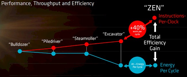
With the Zen cores, AMD had the ambitious goal of keeping the energy efficiency per clock cycle the same as with the Excavator cores, but to boost the amount of work done per cycle by 40 percent or more. AMD also wanted to do a few other things, such as adding simultaneous multithreading (SMT) to its cores to compete with Intel’s HyperThreading, both of which provide two virtual instruction pipelines per core to operating systems, allowing them to interleave more instructions and data and get more work through the chip in a set amount of time provided that the workloads running on the machine are reasonably heavy threaded. There are a lot of architectural changes with the Zen core design, but many of the main ones that server makers and buyers are worried about were confirmed this week by AMD.
First, as we had heard last summer, Naples does indeed have a total of 32 cores per socket. This is not a monolithic chip that has 32 cores etched on it, but rather is comprised of multiple chips, each with one or possibly more of the compute complexes, or CCXs in the AMD lingo, assembled edge to edge and linked as if they were one big chip. The benefit of using this multichip module approach is economic. The yields on a small chip are much higher than on a larger one because the odds of a failure grow with the size of the chip. By ganging up multiple chips in a single socket, vendors such as AMD, IBM, HPE, and even sometimes Intel have been able to boost the performance per socket and lower the cost per socket than it might otherwise be. Here is what the die shot of the Ryzen desktop processor announced last week by AMD looks like:
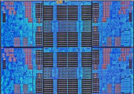
This die shot shows an eight core desktop chip that is comprised of two of the CCX structures, stacked on top of each other, with the areas in blue each having two Zen cores. As you move in towards the center away from the cores, you go through the L2 cache controllers, the L2 cache at 512 KB per core, the L3 cache blocks at two per core of 1 MB each, with a stripe of L3 cache controller circuits through the center of the L3 cache segments and linking them together. AMD could be making each CCX individually for all we know, and putting multiples into each processor socket, but we think it is using an eight-core chunk as its basic building block. That means the Naples chip has four of these in a single socket, yielding 32 cores and 64 threads. In other documentation we have seen, AMD calls this approach “die-NUMA” and says further that Naples scales its performance in this fashion:
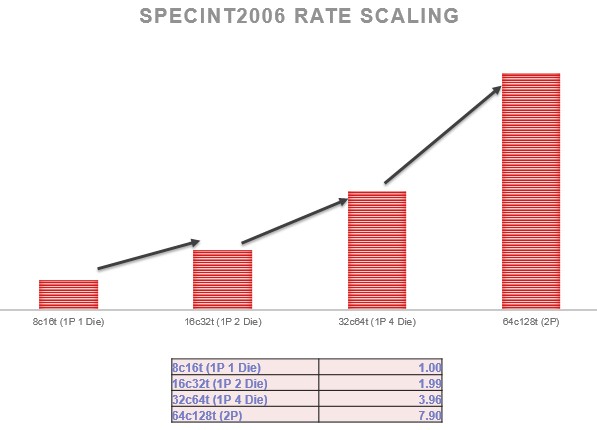
The notes that Mark Papermaster, AMD’s CTO, had in his Ryzen presentation last week at the desktop launch sort of give away that Naples has four chips per socket in addition to talking about the linear scaling of integer performance using this approach: “Naples with its die-NUMA should scale near perfect when you go from 1-Die to 4-Die in a 1P system and then from 1P –> 2P. We are still validating these expectations with our B1 silicon but the results thus far are tracking well. These are estimates on how SPEC_int_rate would scale with core count. Not reported directly from a test but rather derived from test results that are reported from runs at each core count. We do not yet have silicon measurements to confirm these.”
As we previously reported in discussing the prospects for Naples with Forrest Norrod, senior vice president and general manager of the Enterprise, Embedded, and Semi-Custom group at AMD. Norrod tells us that AMD expects that its SPEC_int_rate integer performance of a 32-core Naples processor to be on par with the 28-core top bin “Skylake” Xeon part coming from Intel around mid-year. We have no idea what the clock speed on the Zen chips will be, but if history is any guide, then a good guess is that a 28-core Skylake Xeon chip will run at around 1.8 GHz, considerably slower than the top bin 22-core “Broadwell” Xeon that is etched in the same 14 nanometer processes by Intel. Generally, you trade off higher core count with lower clock speeds and get a net gain in performance within the same power envelope. The only reason X86 chips don’t have hundreds of cores is because certain single-threaded applications still need relatively high clock speeds–something approaching 3 GHz if possible, and 4 GHz would have been better and remember 10 GHz was the goal a long time ago. If Intel and AMD had any sense, there would be two different types of Opteron and Xeon chips: Ones etched with high core counts and a completely different, very specialized design with high clock speeds that was optimized for that. (They both sort of do this, but not really.) But that is a topic for another day….
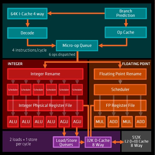
We have detailed the specs of the Zen core already, but it bears some updating. With the Hammer and Dozer cores, AMD worked on frequency and it worked on core scalability, and with the Dozer design it made some compromises in the two-core compute block where not all elements could be used simultaneously and that made it look more like one and a half cores sometimes – and that is another reason why Intel’s Xeons got an edge over the Opteron 6200 and 6300 and most likely why AMD did not even bother pushing hard with an Opteron 6400 and 6500 using the Steamroller and Excavator cores in recent years. With the Zen design, not only can the core do multiple things at once, but it has SMT to fill in the gaps and it was designed to be power efficient from the ground up. The Zen core has a wider and deeper pipeline, has a much improved cache hierarchy, and much better branch prediction, resulting in a much smoother experience.
The Zen core has four integer units (ALUs) and two address generation units (AGUs), plus two load/store units and two floating point units. The core can dispatch six micro-ops per clock instead of four with the Excavator core that never made it into a true serve chip, which might have been called the Opteron 6500 had it come out in 2014 or 2015 or so. The bandwidth on the L1 and L2 caches is double that of the L1 and L2 caches on the Excavator cores, and L3 bandwidth was pumped up by a factor of more than 5X. The Zen core has 64 KB of L1 instruction cache and 32 KB of L1 data cache. Each core also has a 512 KB L2 cache that can store either instructions or data, and each core has a port into a 2 MB segment of a unified 8 MB L3 cache. All the caches are linked by 32 byte ports to the L3 cache and all cores can see all elements of the L3 cache with about the same average latency, which means for all intents and purposes it looks like one big L3 cache. This is why the L3 caches are in the inside of the chip, all close to each other, and the cores are all on the outside – a so-called “cores out” layout.
In addition to these basic functions, the Zen core has some new goodies, which AMD calls its SenseMI features, and the MI stands for “machine intelligence.”
- The Pure Power feature monitors the temperature, clock speed, and voltage of cores and other components and figures out how to optimize them for a given set of performance and the lowest possible thermal footprint, and it does so in conjunction with the Infinity fabric interconnect that is used by AMD to link cores to each other on a die, sockets to each other within a system, and CPUs to GPU accelerators over PCI-Express links now and maybe a point-to-point link sometime in the future. (Why not get PCI-Express out of there?)
- The Precision Boost feature in the Zen cores allows for more than an order of magnitude higher level of CPU clock speed granularity, with 25 MHz stepping, compared to the Excavator cores, and importantly it allows for on-the-fly clock adjustments up and down without halts or queue drains.
- The Neural Net Prediction, which AMD says is “scary smart,” is literally a baby neural network running inside of the Zen core that builds a model of branch predictions based on actual running code and anticipates what future code will need and then pre-loads data and determines the best path through the Zen processors for the data and instructions to most efficiently get the work done.
- Smart Prefetch watches data access paths into and out of the processor and anticipates what will be needed to be pulled into the L3 cache ahead of time based on the applications that are running.
What is the effect of all of these changes to the microarchitecture? We have to infer them from the Ryzen desktop chip, but they will apply equally well to the Naples server chip. Here is how they all stack up:
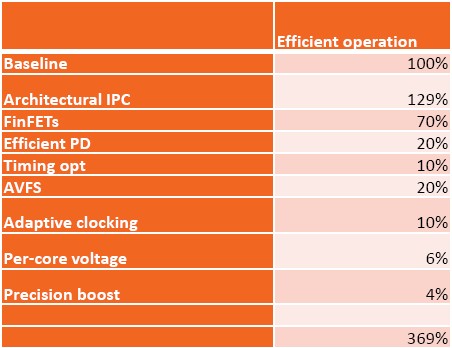
These IPC and energy efficiency improvements are measured using the Ryzen R7 1700 processor, which has eight cores and a thermal design point of 65 watts and is gauged using the Cinebench nT benchmark test, which is really aimed at desktop workloads not servers, but it gives us an idea. The architectural and IPC changes yield the best jump in performance per watt compared to the Excavator core – 129 percent in total, with 52 percent coming from IPC alone and better than the 40 percent target of the Zen core design – and the shift to 14 nanometer processes yielded another 70 percent boost over the Excavator. Another 40 percent comes from Pure Power microfine clock scaling, and another 31 percent from the physical design (we think cores out layout of the chip block and changes in the cache hierarchy are a big part of this), and when you add it all up, you get a 270 percent improvement in performance per watt of a Zen core compared to an Excavator core. Granted, this is over a many-year period. But it is still impressive.
Weaving It All Together
The other important new feature is that Infinity fabric interconnect, which is a kind of HyperTransport on steroids and one that will, we presume, be more easily extended out to other CPUs, GPUs, and possibly FPGA accelerators in the future. Infinity fabric is for what happens inside of the box, not between boxes, although InfiniBand and Ethernet fabrics, as well as PCI-Express switches, can be used to lash boxes together, and AMD is involved with both the CCIX interconnect, Gen Z interconnect, and OpenCAPI interconnect efforts, so all kinds of interesting things are possible in the future.
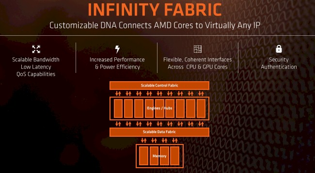
The details on this fabric are not being divulged at this time, but the same circuits that are used to create PCI-Express lanes are being used to implement this fabric to link two Naples sockets together. Papermaster says that Infinity is a coherent HyperTransport interconnect plus enhancements, which has low latency and bandwidth and power consumption that are malleable, scaling up and down as needed, rather than being static. The feeds and speeds have not been divulged, but we can infer some things.
The Naples chip is a true system on chip, Dan Bounds, senior director of enterprise products at AMD, tells The Next Platform. That means, among other things, that it does not require a southbridge chipset, as Xeons do, to talk to external I/O devices. This streamlines the server design and cuts costs; Skylake Xeons are socket compatible with Broadwell Xeons, so they will not be an SoC design. Yet another advantage that AMD will have as the Naples chip comes to market, adding to the ones we have already discussed in our previous story.
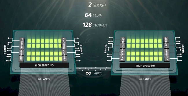
As you can see in the Naples platform diagram above, a two-socket Naples system has 64 lanes of PCI-Express I/O coming off each socket. As it turns out, each Naples chip has a total of 128 PCI-Express lanes, and in a single-socket system all of them can be dedicated to running traditional I/O devices. In a two-socket setup, half of the lanes are used to cross-link the sockets to each other so they can provide a single computational substrate and a unified memory address space using NUMA techniques. On single socket machines, all of those 128 I/O lanes can be used to hook to external I/O. Bounds tells us that the Naples chips were optimized for systems with one or two sockets only, and further that the company has no plans to support four-socket or larger systems. And it is immediately obvious why this is the case. If AMD wanted to make a four-socket machine, it would have to use all 128 lanes to crosslink the sockets, and to do it right with all processors being only one hop away from each other, it would need 192 lanes for a four socket with one hop between processors, and an eight-way would require at least 256 lanes and would still have some sockets two hops away from each other.
This doesn’t matter much, since machines with one or two sockets address all but the very high end of the market, where the shipment volumes are low even if the profits are very much higher than in the two-socket space. AMD has to pick its targets, and if need be, it can create a server chip with more I/O and an extended Infinity fabric to go after this high-end NUMA market if it needs to.
As you can see in the chart above, the Naples processor has a total of eight memory channels (one per Zen CCX unit, we think), and each channel support two DDR4 memory sticks. So that is up to 16 memory sticks for a single socket machine and up to 32 sticks for a two-socket box. Here is how the Naples system will stack up to a current Broadwell Xeon system using the top-bin 22-core E5-2699A v4 processor:
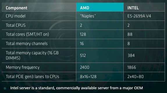
As you can see, AMD will have the advantage in terms of cores and threads, and with twice as many memory channels it will also have a memory bandwidth advantage. On Naples machines it has tested, AMD can push 170.7 GB/sec of memory bandwidth, compared to Intel’s 76.8 GB/sec on its own tests using a Broadwell system with the top bin parts. Intel Broadwells can have up to three memory sticks per channel, compared to two for Naples, so the Naples chip tops out at 512 GB using very cheap 16 GB sticks compared to 384 GB for the Broadwells. So that is a 122 percent memory bandwidth and a 33 percent memory capacity advantage to AMD. (The Naples chip can also run the memory at 2.4 GHz compared to 1.87 GHz for the Broadwells, and that 29 percent speed bump is why it has higher bandwidth than the memory subsystem on the Xeon chip.) If you need to maximize memory in either a Naples or Broadwell system, the former tops out at 2 TB while the latter maxes at 1.5 TB in two-socket machines.
AMD also has the advantage when it comes to I/O, with 128 lanes of traffic for either single socket or dual socket machines, compared to 40 lanes per socket for Haswells and Broadwells. The Naples chip is sticking with PCI-Express 3.0 lanes, which deliver 985 MB/sec of bandwidth per lane in each direction, rather than moving up to PCI-Express 4.0 lanes, which will double that up to 1.97 GB/sec of bandwidth. The Broadwell chips support the same PCI-Express speeds. As far as we knew back in May 2015, when we revealed the specifications of the future Skylake Xeons, Intel was sticking with PCI-Express 3.0 for these chips, but with IBM supporting PCI-Express 4.0 with the Power9 chips and it needing an advantage of some sort over Naples, Intel might have gone back and added PCI-Express 4.0 support to the Skylakes.
Here is the issue: You can’t drive a dual-port 100 Gb/sec Ethernet or InfiniBand card from a single PCI-Express 3.0 x8 slot on a server. You need a PCI-Express 4.0 x8 slot. For many hyperscale and HPC shops, this will be important. For most enterprises, not so much. It might be more important to be able to connect lots of PCI-Express devices directly to one or two sockets and eliminate the need for a PCI-Express switch, and this is the tradeoff that Bounds tells us that AMD made.
In terms of performance, AMD gave us a taste of how the Naples server will compare to a current Broadwell server using a seismic analysis workload from the oil and gas industry that does a bunch of Laplacian transforms of 3D wave equations to try to figure out where oil might be lurking in the ground using echoes bouncing off the rocks. This particular workload, says Bounds, stresses the cores, the memory, and the I/O subsystem alike and is representative of many workloads that are running in enterprises. “We wanted to create a scenario where cores matter, but what really matters is the memory, both the bandwidth and the capacity,” explains Bounds.
In the first test that AMD did, it had a 1 billion cell sample grid of data and ran ten iterations of the simulation. It only activated 44 cores on the Naples machine and geared back the main memory to run at 1.87 GHz, just like the two-socket Broadwell Xeon system. It took the Intel box 35 seconds to run the simulation at a rate of 286 computations per second, but the AMD machine could do the simulation in 18 seconds, or just about twice as fast, at a rate of 527 computations per second. In a second run, using the same sample size of 1 billion data points and ten iterations, but with all 64 cores turned on and with the memory boosted up to the full 2.4 GHz speed, the Naples machine was able to do 713 transactions per second on the seismic simulation, and that meant it finished in 14 seconds and was 2.5X faster than the Broadwell machine. (We asked Bounds if this incremental performance boost was helped by the CPUs, and he said that nearly all of it was due to the increased memory speed.) Just for fun, AMD did a third test, quadrupling the dataset size to a 4 billion sample grid, and it could run that in 54 seconds on the Naples box, but it would not even load the data on the Broadwell box.
When it comes to all of the feeds and speeds, AMD is not delusional about how Naples will stack up against the future Skylakes. “We fully realize that Skylake will close this gap, but the gap is still going to exist and it is going to be material. These are still the kinds of numbers we get excited about, especially if you start to think about the implications of having to process big and fast data.”
So here is how the gaps could close. Skylake is expected to top out at 28 cores, so AMD will only have a four core advantage there. It is hard to say what the clock speeds will be, but AMD has told us that integer throughput should be about the same for each socket.
Skylake is expected to have six channels of memory per socket, compared to eight channels for Naples. The Skylake memory controller will allow one stick per channel running at 2.67 GHz and two sticks per channel running at 2.13 GHz or 2.4 GHz. So Naples will have the capacity and bandwidth advantage to the tune of 33 percent on a Skylake socket with twelve sticks. As for I/O, Skylakes will offer up to 48 lanes of traffic per socket and support the PCI-Express 3.0 protocol, up by 20 percent compared to the Broadwell Xeons, but Naples will still have a 33 percent I/O lane and bandwidth advantage – unless Intel switches to PCI-Express 4.0 and/or adds more lanes. Neither is easy, but neither is impossible, either.

He Who Can Pay Top Dollar For HBM Memory Controls AI Training
What is the most important factor that will drive the Nvidia datacenter GPU accelerator juggernaut in 2024? Is it the forthcoming “Blackwell” B100 architecture, which we are certain will offer a leap in performance over the current “Hopper” H100 and its fat memory younger sibling, the H200? No. Is it …

Energy Efficiency Pays Its Way In The Datacenter
SPONSORED POST Over the past decade, the heat generated by server CPUs has increased by 3.5X and now is pushing 500 watts. GPU heat is up by 3X to 700 watts, typical server DRAM memory is up by 4X to just shy of 300 watts, and network adapters are up by …
Intel To Broaden FPGA Lineup And Make Them At Home
Back in 2015, when Intel was flush with cash thanks to a near-monopoly from X86 datacenter compute, it shelled out an incredible $16.7 billion to acquire FPGA maker Altera because a few hyperscalers and cloud builders were monkeying around with offloading whole chunks of CPU compute to FPGAs to create …
The 28-core number is the one from the leak 2 years ago. More recent leaks have pointed at 32-core SKUs, which may or may not have been because of Naples.
Further, all these comparisons are utterly irrelevant since Naples will go up against Skylake-EP. I hope to see a side-by-side comparison when Intel announces SKX.
The 32c skews are for E7 not E5 and will likely still be at an I/O and Memory disadvantage.
Sku
Well hard to tell. If AMD delivers on what they have been showing so far they have a very good chance to be back in the game. And congratulation to that it is a lot better than I would have expected.
What actually might kill them though is no AVX-512 support. So if these Simulation guys actually recompile their code with AVX-512 support that 2 times performance will vanish pretty quickly and might actually turn in the other direction easily.
Yes there are curiously 4 of the exact same dual CCX Unit(8 cores total per die) dies used to scale up to 32 cores for the Naples on MCM SKU. And this appears to me to be exactly what is used to make up the one dual CCX Unit(8 cores total) die for the Ryzen 7 series consumer variants. So Naples is Ryzen times 4 with some extra IP and more infinity fabric width enabled for the Naples 4 die based MCM SKU.
So Ryzen appears to be in actually ¼ of a Naples with that wafer yield much better for using that Dual CCX(8 cores total die) in the making of the modularly scaled up Naples Server MCM SKU. AMD is Very Smart in designing things this way and the next GPU generation from AMD, after Vega arrives this year, Is the Navi design that is expected to be made in a modular fashion from few up to many modular smaller GPU chiplets, for the very same die yield and scalability advantages of using smaller dies to increase the usable die/wafer yields in the making of any multicore processor variants.
Very smart move AMD,! For much better yields and the scalability of design advantage that comes from modular methods on the MCM or the Interposer(future SKUs)
“The details on this fabric are not being divulged at this time…”
I would suggest the fabric is the same “Freedom Fabric” ASIC that AMD acquired along with “Sea Micro”. Which evidently may have been the reason for that acquisition in the first place. Quite a bit of AMD commentary was centered around the use of this particular ASIC.
“AMD is taking a $75 million writeoff against the SeaMicro assets, but CFO Devinder Kumar said that the intellectual property of the Freedom Fabric interconnect “is still available for us as needed.” That does not sound much like a plan to add proprietary interconnects to future Opteron X86 and ARM server processors.”
https://www.nextplatform.com/2015/04/17/amd-hits-reset-on-server-business/
“AMD Talks Next Generation Coherent Interconnect Fabric Connecting Polaris GPUs, Zen CPUs and HPC APUs”
http://wccftech.com/amd-coherent-interconnect-fabric-gpus-cpus-apus/
So, it looks like this will be launched in summer. I’m wondering if they will have the server parts ready to go at launch, or will OEMs need a few months to design their products around Naples?
Also, I noticed during the Ryzen 7 launch a lot of games and applications didn’t perform as well as they should because they weren’t optimized to work with Ryzen. I’m wondering if the same thing is going to happen for Naples
In the seismic workload, running the memory at 2.4GHz instead of Intel-equivalent 1.87 GHz improved the result from 18 seconds to 14. This is *exactly* the same ratio (down to 0.2%). This suggests the scenario may be entirely memory-limited and unleashing all 64 processors rather than the Intel-equivalent 44 made no difference.
I disagree, read https://www.theregister.co.uk/2012/03/20/amd_launches_opteron_3200_server_chips/
Friendly, Shavonda