
The server space was a-buzz this weekend with what looks like a big leak of Intel’s future Xeon processor and chipset roadmaps for the next couple of generations of machines. The roadmaps, which are not as polished as the final ones tend to be, seem plausible even if Intel has not confirmed the data is real and very likely will not. So take this all with a fairly large grain of salt.
It is fun to consider the Xeon roadmap outage anyway, especially in light of the recent moves by AMD to boost its Opterons with a new “Zen” architecture and its commitment to re-enter the server market with a certain amount of gusto. Whether planned or not, the leak, if the data turns out to be true, shows that AMD will have a hard time displacing Xeon gear from datacenters – something that was not as true with the original Opterons from a decade ago when Intel was distracted and left itself open for competition.
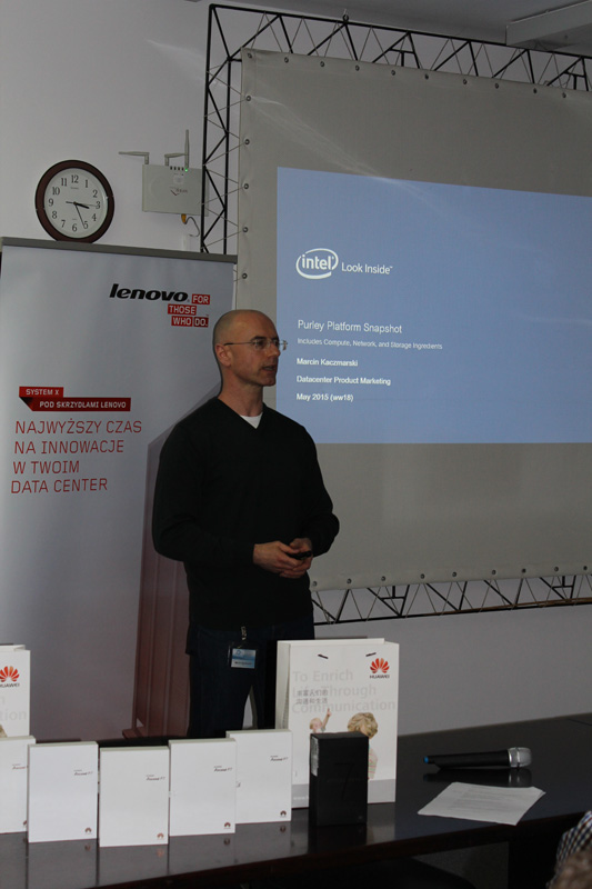
Here is the link where this supposedly authentic Xeon and Xeon Phi roadmap, running from 2015 out through 2017, is posted. The slides were created in English and the link to them goes to a domain owned by the Konferencji Użytkowników KDM (that means HPC User Conference in Polish), which Intel participated in from May 11 and 12. By the time you read this, the PDF file with the roadmap will no doubt be removed. (But, then again, maybe not if the cat is truly out of the bag as it looks like it is.) The fact that there is a photograph with someone standing in front of the first slide of the Intel deck makes us think this is a real presentation and one given by Marcin Kaczmarski, who runs datacenter product marketing in Poland, as the slides suggest:
The presentation given by Kaczmarski focused on the future “Purley” server platform, which is being created to run future “Skylake” family Xeon processors. The roadmap revealed the brand names that Intel will be using for future “Knights Landing” Xeon Phi massively parallel processors but less than we have already revealed about these future 72-core processors and their on-die Omni-Path interconnect.
The interesting bits of this roadmap reveal have to do with impending “Broadwell” Xeon processors for two-socket and larger systems that are expected to roll out later this year and into next year and the Skylake Xeons expected perhaps a year later. Intel started rolling out Broadwell client chips last year and put the first server variant, the Xeon D, into the field back in March. Broadwell-EP processors are expected in the late summer at Intel Developer Forum for two-socket machines, and to be followed by Broadwell-EX processors for four-socket and larger systems and a Broadwell-EP variant aimed at entry four-socket systems that sits between the two. The roadmap that Kaczmarski showed is consistent with what we expected Intel has done since last year and what we expect it to do in the coming year:
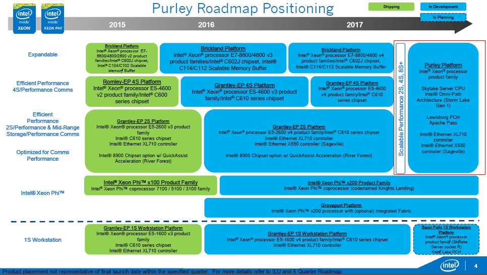
The timings are not precise, obviously. The “Grantley-EP” platform using the Xeon E5-2600 v3 processor, which is also known by the code-name “Haswell-EP,” actually debuted in September 2014. The “Brickland” platform, which has four or eight sockets using the E7-8800/4800 processors (also known as the “Haswell-EX”), was just announced in early May, and we are expecting for the four-socket variant of the “Haswell-EP” chip, known as the E5-4600 v3, any week now. In the blue boxes in the roadmap above, any of the machines labeled with “v4” in their names are based on the Broadwell kickers to the Haswell cores and etched using 14 nanometer processes compared to the 22 nanometers used with the Haswells. With the future Skylake Xeon processors, Intel will hold the process constant at 14 nanometers and do more work on the microarchitecture to goose performance. A kicker to Skylake, code-named “Cannonlake” if the rumors are right, will shrink the Skylake cores down to 10 nanometers.
The interesting bit about this roadmap chart above is that it seems to suggest that Intel will be converging its two-socket and four-socket Xeon E5 platforms with its four-socket and eight-socket Xeon E7 platforms, which have been separate up until now, into one platform called Purley, presumably after the neighborhood in south London in England. The idea of the Purley platform, as Kaczmarski’s presentation puts it is that it “provides significant performance combined with a rich feature set based on cutting edge technology resulting in compelling benefits across a broad variety of usage models.” The Purley platform will have processor SKUs and platform variants that are aimed at HPC, enterprise, cloud, storage, and networking workloads. These are the key markets for CPUs at Intel, of course.
This chart has some interesting goodies on it:
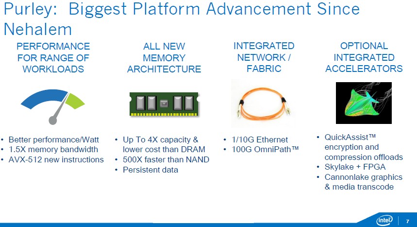
For one thing, the Skylake processors will sport the 512-bit AVX-512 vector processing units that are making their debut in the “Knights Landing” Xeon Phi processors that are expected to launch in the second half of this year. (The roadmap above puts Knights Landing into 2016, and that may be when true volume shipments start. Intel has said it will ship the Knights Landing chips for revenue this year, but it often ships Xeon and Xeon Phi processors ahead of a formal launch to key hyperscale or HPC customers. So the difference between what Intel has said and what this supposed roadmap above says is not an inconsistency.)
The idea that the Skylake chips used in the Purley platform would yield 1.5X the memory bandwidth is not surprising, and this will apparently be accomplished by having six channels per socket compared to four channels per socket for prior Xeons. The talk of “an all new memory architecture” that has 4X the capacity (to a maximum of 6 GTB for a two-socket system) and lower cost than DRAM that is 500X faster than NAND flash memory and allowing for persistent data certainly caught our attention.
It is not surprising that these future Skylake Xeons will have 10 Gb/sec Ethernet or 100 Gb/sec Omni-Path fabrics integrated on their dies, and that Intel will offer variants with FPGA or GPU accelerators as options is also not unexpected. The roadmap notes also say that Xeon and Xeon Phi compute nodes will have a “converged programming environment” with “compute and I/O nodes linked through a common fabric.” Some variants of the future Skylake Xeons will have four 10 Gb/sec Ethernet interfaces integrated into the Intel chipset for the processors, and these interfaces will support Remote Direct Memory Access (RDMA) using the RoCE protocol that is becoming more popular among hyperscalers, cloud builders, and HPC shops that tap Ethernet instead of InfiniBand for low latency.
Here is how a typical two-socket Purley machine with Skylake Xeon E5-2600 v5 processors might line up:

You will notice a few things in here. First, look at all of those networking options. Second, there is a new interconnect called UPI, presumably for Universal Path Interconnect or some such, that is a kicker to the QuickPath Interconnect that has linked processors to each other for NUMA clustering since the Nehalem generation was launched in 2009. (“Storm Lake” is the code-name for the Omni-Path 1 fabric ports and the free-standing interface cards Intel will also make so Omni-Path interconnects can be used with chips other than Intel’s own Xeon and Xeon Phi products.)
Here is a table that shows how the converged Purley platform based on Skylake Xeon v5 processors will stack up to the Grantley platforms using Broadwell-EP Xeon E5 v4 processors and Brickland platforms Broadwell-EX Xeon E7 v4 processors.
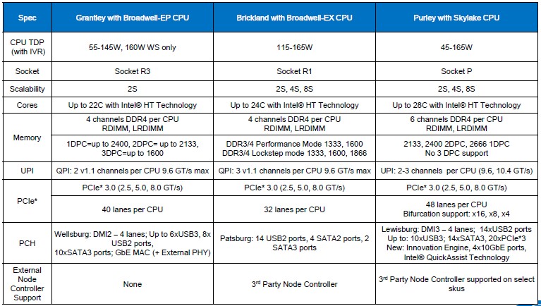
Remember, Intel skipped “Sandy Bridge” with the Xeon E7s, which is why the version numbers don’t match for Broadwell chips in the table above.
The big reveal are the top-bin core counts for the Broadwell and Skylake processors, with the Broadwell Xeon E5 v4 topping out at 22 cores (up from 18 with the Haswell-EPs) and the Broadwell Xeon E7 v4 coming in at 24 cores (up from 18 cores with the Haswell-EXs). The Skylake Xeon v5 (maybe there will be Xeon E5 and Xeon E7 variants, maybe not) will top out at 28 cores. This is considerably more than the 16 cores that AMD is rumored to be putting on a single die for its future Zen Opteron processors.
It is interesting to note that the Skylake chips are supporting DDR4 memory, so whatever this revolutionary new memory architecture is, it includes DDR4 running with two DIMMs per channel at a slightly higher clock speed than will be available on the future Broadwell-EP chips. The UPI interconnect between the processors will have two or three channels per processor socket, which is consistent with QPI ports of the Xeon E5 (two) and Xeon E7 (three) chips; the speeds of the UPI ports run at 9.6 GT/sec or 10.4 GT/sec, which is not much different from the top speeds available with QPI today. What makes UPI different from QPI is not clear, but it may have to do with a slightly more efficient protocol that can also be extended out to other peripherals such as flash or coprocessors such as FPGAs. This is what IBM has essentially done with its Coherent Accelerator Processor Interface, or CAPI, on the Power8 processors, and Intel was hinting earlier this year that it could modify QPI to speak to things other than Xeon sockets. The Skylake chips do not have PCI-Express 4.0 peripheral links, and with the networking built onto the chip, there might not be a big rush to add it should the specification be ready by 2017 or so.
There is a lot to chew on here. And we intend to do just that. Share your thoughts.

How High-Bandwidth Memory Will Break Performance Bottlenecks
Intel recently announced that High-Bandwidth Memory (HBM) will be available on select “Sapphire Rapids” Xeon SP processors and will provide the CPU backbone for the “Aurora” exascale supercomputer to be sited at Argonne National Laboratory. Paired with Intel’s Xe HPC (codenamed “Ponte Vecchio”) compute GPUs running in a unified CPU/GPU …
3D XPoint Memory At The Crossroads
Like many system architects the world over, we had high hopes for the 3D XPoint variant of phase change memory (PCM) when it launched with much fanfare back in July 2015 after being developed jointly by Intel and Micron Technology for many, many years. This represented a new kind of …
Intel Sometimes Charges A Hefty Premium For Sapphire Rapids
No matter what, and without any excuses about Moore’s Law slowing down, those buying compute, storage, and networking expect at least one thing in any generational leap in a device: That the cost per unit of capacity goes down. And for the hyperscalers who run massive applications, they look at …
New memory:
– persistant
– 500x faster than NAND
–> Phase-Change-Memory?
I guess we will see 4-way SMT with Skylake-EP?
So basically Intel will catch up to Fujitsu’ Primehpc FX100 in a few years.
You appear to be right that that information has been yanked. The link takes us to a page in Polish, which when translated to English via a on-line translation tool, reads “It looks on it, that has nothing here. Is proper to search for it can? “
just trying to see what the next SQL geared CPU’s will be. looking for 8889 V4 cpu specs. want to know highest clock speed and lowest number of cores. (6 CORES in the high 3.5GHZ would be great)