

We have been saying for the past two year that the impending “Skylake” Xeon processors represented the biggest platform architectural change in the Xeon processor business at Intel since the transformational “Nehalem” Xeon 5500s that debuted back in March 2009 into the gaping maw of the Great Recession.
There is no global recession breathing down the IT sector’s neck like a hungry wolf here in 2017, eight years and seven chip generations later. But Intel is facing competitive pressures from AMD’s Naples Opterons, IBM’s Power9, and the ARM collective (mainly Cavium and Qualcomm at this point, but Applied Micro is still in there), and it is also trying to stretch the Xeon’s across more diverse customers and workloads, and that means the Skylakes warranted something more than just coming out with new cores coming in a refined 14 nanometer process and slapping the Xeon E5 and E7 labels on them. As it turns out, the Skylake Xeons will make a break with the past and change in the way that CPUs – and sometimes adjacent accelerators for compute and network – will be engineered and sold.
The Wall Between DP And MP Comes Down
For as long as Intel has been peddling processors for the datacenter, it has chips aimed at different segments of the market, starting with the “Foster” generation of Xeons back in 2001, which came in DP variants for two-socket servers and MP variants aimed at four-socket boxes. Intel sold processors for two-socket machines before then, but allowing greater SMP scalability required different chipsets (often done by third party chipset makers but also by Intel) and changes to the cache structure on the die as well as different ratios of cores, cache and main memory, and peripheral I/O as these were all scaled up by Moore’s Law manufacturing advances.
In the mid-2000s, Intel broke the server processor line into three chunks, with the Xeon 3000 series being aimed at single socket machines, the Xeon 5000s being aimed at machines with two sockets, and the Xeon 7000s for machines that had four sockets and sometimes more with the help of third party chipsets. These divisions more or less correspond to the current Xeon E3, E5, and E7 categories that Intel has used since the Nehalem days but which became a regular, predictable pattern starting with the “Sandy Bridge” Xeon processors. Sometimes Intel offered versions of the E7 that scaled down to two sockets as well as to four or eight sockets or E5s that scaled up to four sockets to address specific needs – the latter for a cheap, dense virtualization and database engine. But generally, this pattern has held. Intel has then offered specific tweaks within the E5 and E7 groups that had fewer cores and higher clock speeds or more cores and lower clock speeds than the standard parts, and indeed, within the latest several generations of the E5 there are multiple distinct chips. With the “Broadwell” generation for instance, there are three different E5 chips that top out at 10, 15, or 24 cores on the dies as well as a single E7 chip with a maximum of 24 cores; the E7s are more ruggedized and have memory subsystems that have buffer chips on them to support large main memory and high bandwidth.
With the Skylakes Xeons, Intel is doing one important thing that will make life easier for both server makers and their customers, and it is something we told you about two years ago. And that is that it is moving from two distinct motherboard sockets – the Socket R3 aimed at dual-processor Haswell and Broadwell Xeon E5s and the Socket R1 aimed at the Haswell and Broadwell Xeon E7s – to a single Socket P that will be used by all of the Skylake Xeons that might otherwise have been given the Xeon E5 and E7 brands. By moving to a single socket design, motherboard makers will be able to design fewer motherboards to support what we presume will be a more diverse set of processors, and this should cut costs for all parties – from motherboard makers to system sellers to end user customers.
This converged Xeon E5 and Xeon E7 platform, as we have discussed in the past, is code-named “Purley” by Intel, and it will scale from two sockets up through four and on to eight without requiring any external chipsets from third parties. (It is not clear if third parties will make chipsets to scale out Skylake Xeons beyond eight sockets, but rest assured we will find out.) From what we know, the Skylake Xeons will top out at 28 cores, and as best we can figure, this is what the top bin part will look like:

Starting with the Skylake Xeons, which will be called the Xeon Processor Scalable Family, there will be four distinct flavors of Xeon processors, and the chip maker is going Olympic and then some on its naming conventions:
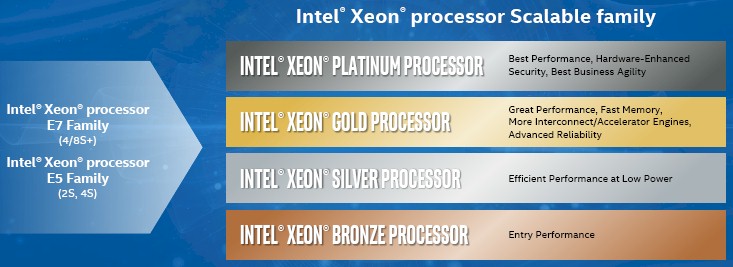
It would be tempting to think that these four different categories – Bronze, Silver, Gold, and Platinum – will roughly correspond to the three different Xeon E5 variations – Low Core Count, Middle Core Count, and High Core Count as they are called internally – and one Xeon E7 variant that we have seen in the past. Intel is not saying precisely what features will be on what metallic level of the Skylake Xeons, but what we know for sure is that the Skylake cores in this Xeon Scalable family will support larger on-chip L1 and L2 caches per core as well as the normal bump in L3 cache size that comes with a redesign. Lisa Spelman, general manager of the Xeon Products and Datacenter Marketing Group at Intel, tells The Next Platform that the Xeon E3, which was upgraded to the Skylake cores more than a year ago and which was just recently upgraded to the Kaby Lake cores, and the Xeon-D system on chip that was created for hyperscalers that is an amalgam of sorts between a Xeon E3 and Xeon E5 chip, will remain distinct from this converged Xeon E5 and E7 family. As far as we know, there will be no formal single-socket version of these Skylake Xeons, but there will be nothing that will prevent a motherboard maker from creating a single socket board if they want to sell it.
Spelman also confirmed that the entire Skylake family – meaning all four variants of what is called the Skylake-SP to distinguish it from the Skylake-H used in the Xeon E3 v5 family – would launch at the same time, and that there would not be a staggered rollout as we have seen in the past, with the two-socket Xeon E5s coming first, followed by the Xeon E7s, and then the four-socket Xeon E5s.This is good for a number of reasons. For one, server makers and buyers will be able to select the systems that meet their very precise needs right then, and not have to guess what might be coming down the pike in the rest of the family. This will also help Intel get on an annual cadence for both processor generations and process iterations, something that the company has said it wants to do and something that is necessary if the Xeon server chips will move to the front of the process line, as is the plan starting with the 7 nanometer manufacturing ramp.
Intel has a lot of different toggles it can switch on and off within this Skylake-SP processor family to generate a wide and deep SKU stack, and we expect it to do just that. Intel can ramp the cores up and down and turn HyperThreading on and off as it has done in the past. As far as we know, each Skylake-SP chip has six channels of DDR4 memory per socket, with registered and load-reduced DIMMs as options. The processor will support 2.67 GHz memory with one DIMM per channel and 2.13 GHz or 2.4 GHz at two DIMMs per channel; three DIMMs per channel, which was supported on the prior “Grantley” server platform based on the Haswell Xeon E5 v3 and the Broadwell Xeon E5 v4 processors, is not available on the Purley. Intel could distinguish the Bronze, Silver, Gold, and Platinum processors in the Skylake-SP Xeon family by memory speed as well as the number of DIMMs supported. The Bronze entry performance chips could have support only for slower memory, and less of it, while the Platinum versions aimed at high performance could have the fastest memory and more of it. It is not clear if Intel is keeping the buffered memory that has been part of the Xeon E7 architecture but not in the Xeon E7. Spelman did not reveal Intel’s plan here. This is an annoyance to add to the server platform, but it does allow for main memory to scale up on large four-socket and eight-socket NUMA machines. What is clear from what Intel has said is that the Skylake Gold processors will have fast memory, more interconnect and accelerator engines, while the Skylake Platinums will have the highest performance (by which Intel no doubt means throughput) as well as hardware enhanced security.
Our guess is that there might be three different versions of the Skylake-SP chips, roughly corresponding to the Xeon E5 LCC, MCC, and HCC variants and that Intel has actually collapsed the Xeon E5 HCC and Xeon E7 capabilities into the Skylake Platinum variant. The Gold and Platinum chips are distinguished by which features are turned on and off with the Skylake die and the broader Purley platform.
For instance, it is not a foregone conclusion that the AVX-512 vector instructions, which made their debut with the “Knights Landing” Xeon Phi processor last year and which doubles the floating point performance of each core, will be included on all variants of the Skylake-SP chips. That said, machine learning inference is still largely done on CPUs, not GPUs or FPGAs, and this will be important for the hyperscalers as well as for the HPC crowd. Some variants will have integrated Omni-Path network controllers or FPGA accelerators (over time), for instance; all will have integrated 10 Gb/sec Ethernet controllers. It looks like the top-bin Platinum parts will have integrated QuickAssist encryption and decryption engines.
In general, there is a rough correlation in socket count with the different Skylake-SP variants, too. The Bronze level has two-sockets, and Spelman says this might be used in a storage controller or as a Web server, while the four socket and above machines will be based on the Platinum variant. Intel is moving to a technology it calls UltraPath Interconnect, or UPI, with the Skylakes, which is an upgraded version of the QuickPath Interconnect that links sockets to each other in a NUMA shared memory setup that made its initial debut back with the Nehalem Xeons in 2009.
As far as we know, each Skylake-SP chip will have two or three UPI channels, running at 9.6 GT/sec (same as the top end Broadwells) or a faster 10.4 GT/sec. You burn two channels to make a tightly coupled two-socket NUMA system or to make a slightly less tightly coupled four-socket server and you burn three channels to make a tightly coupled four-socket box or a slightly less tightly coupled eight-socket machine.
If the design has not changed, then each Skylake-SP has a pair of PCI-Express controllers that together have 48 lanes, and two years ago, this was supposed to be at PCI-Express 3.0 speeds but Intel may have pushed to get PCI-Express 4.0 speeds in here. Intel could crimp some of the lanes on the lower-end Skylake-SP chips to encourage those with more peripheral expansion to move up the stack. We shall see.
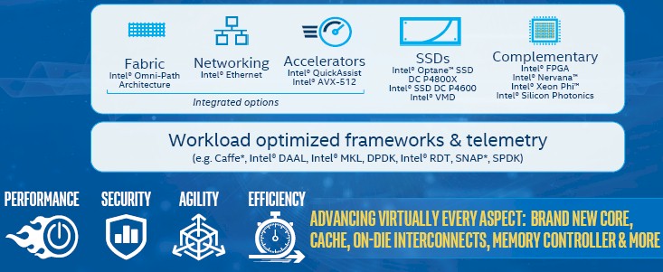
The Purley platform will build out from here with flash and Optane 3D XPoint memory as well as external FPGA and Nervana neural networking co-processors, and the Xeon Phi is thrown in for good measure, too.
It will be interesting to see if the aggregate SKU count goes up, down, or sideways by moving to this new way of packaging Xeon chips for the core datacenter workloads. In the past, Intel has dozens of SKUs that it sells into the broad market, plus additional custom SKUs that it does for hyperscalers, database makers, and HPC shops that need some further optimization to minimize their total cost of ownership.
“We took this opportunity to be thoughtful about our SKUs,” says Spelman. “We don’t want a never-ending explosion of SKUs. We are always looking at what is being accepted by the market and then cull the line. But when you do start to add in new integrations, like Omni-Path, those are net new SKUs even if you have managed down the rest of the product line. So don’t expect to see a dramatic difference, but don’t expect to see an explosion.”
There will still be custom variants that do not end up on the official price list, by the way, because Intel still wants to not leave this engineering and money on the table.

Intel’s Datacenter Decline Not As Bad As Expected
Incoming chief executive officer and long-time Intel employee Pat Gelsinger is talking the helm of a chip company that has plenty of issues to sort out, but there is some good news as Intel reports its financial results for the fourth quarter of 2020 and Gelsinger gets ready to take …
Talking Silicon Photonics Signal And Noise With Andy Bechtolsheim
There is a lot of chatter this week about optical communications with the OFC2022 conference being held in San Diego. We have more than a passing interest here at The Next Platform in silicon photonics and co-packaged optics, and had a chat with Andy Bechtolsheim about what was happening in …
Crunching Photons And Electrons Down Into Datacenter Switch ASICs
At some point, Moore’s Law increases in performance are going to hit a wall when it comes to datacenter networks. But we are not there yet, and the research and development work is progressing so that just about the time switch and router ASICs hit a wall, we should have …
Be the first to comment