
After its acquisitions of ATI in 2006 and the maturation of its discrete GPUs with the Instinct line from the past few years and the acquisitions of Xilinx and Pensando here in 2022, AMD is not just a second source of X86 processors. Now, without question, it is a formidable supplier of high performance computing for all kinds of workloads and within all layers of the compute and interconnect infrastructure in the datacenter.
This has utterly transformed the company, work that took a decade and a half but was only accomplished under the stern guiding hand of chief executive officer Lisa Su, assisted by the very talented team she put together.
That team included Mark Papermaster, chief technology officer; David Wang, senior vice president of engineering for the Radeon GPU group; Jim Keller, who returned to AMD to help out for a stint to get the CPU designs in order before doing the same at Intel and then also leaving to join Tenstorrent; Forrest Norrod and general manager of its Data Center Solutions group; Rick Bergman, executive vice president of its Computing and Graphics group; and now Dan McNamara, general manager of its server business (who formerly ran the Altera FPGA business at Intel) and Victor Peng, president of its Adaptive and Embedded Computing group who has been running Xilinx since 2017 and who ran the GPU business at AMD in the wake of the deal to buy ATI.
Now Prem Jain and Soni Jiandani, serial entrepreneurs who along with Mario Mazzola and Luca Cafiero created the Nexus family of switches and the UCS converged server-networking platform for Cisco Systems, are joining AMD through the Pensando deal.
After five long years of laying out its roadmaps for CPUs and GPUs, with both getting architecturally better with successive generations, coupled with an absolutely steady and predictable launch cadence, AMD has four roadmaps to cover the datacenter, which are themselves overlapping and reinforcing to each other. And now, most people believe AMD when it says it is going to do something. There are still some doubters after the Opteron CPU shutdown and the SeaMicro false start in the early 2010s, but frankly, AMD’s record in the past five years of promising and delivering is far better than what Intel has been able to do. And that is the main reason why AMD is forecasting huge revenue and profit gains in the coming years, as we covered in the wake of the Financial Analyst Day 2022 event last week.
This week, as we promised, we are going to talk about the roadmaps that will drive AMD to technological and financial altitudes it has always dreamed about in the datacenter – and has never been able to ascend to in its long history.
AMD’s success in its second run at datacenter compute starts with a decent amount of money to invest, and a tight focus on putting a competitive CPU and then a competitive GPU out there, which builds enough financial momentum to invest in broader and deeper roadmaps and to do acquisitions like Xilinx and Pensando. (By the way, we do not think that AMD will try to eat other companies – perhaps a young networking company or some software to add to its converged ROCm and Vitis stacks.)
As Papermaster showed in his keynote at last week’s FAD 2022 event, the company has invested in its engineering staff and its research and development budget as it has grown:
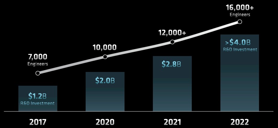
AMD’s R&D budget in 2022 is expected to be around the same size as the entire revenue stream of the company back in 2016, just to give you some perspective. The R&D budget really expanded as AMD built out the CPU and GPU roadmaps in 2020 to take down the exascale HPC deals here in 2022 and 2023, cresting above 20 percent of revenue, and the combination of AMD and Xilinx is settling down to a more typical 15 percent, plus or minus and mostly plus, of revenue here in 2022. That’s the same amount that Google spends on R&D; Facebook spends more at 21 percent of revenues, Apple spends less at around 7 percent, and Intel, which has all kinds of R&D costs that AMD does not in the foundry business and which is playing catchup in a lot of areas, spends about 19 percent.
Between 2019 and 2022, the headcount in engineering at AMD will rise by 2.3X, but the spending is rising by 3.3X. Some of that is due to the spending by Xilinx as it fleshes out its next-generation Versal devices, and there is a very good chance that AMD will start adding software engineers like crazy as it creates a unified ROCm-Vitus platform that doesn’t just span AI (as it is talking about), but brings libraries to bear in traditional HPC and data analytics – just as Nvidia has done. Everything Nvidia has done in terms of libraries and algorithms, AMD must do – and it must do it faster. The fact that it has been done by Nvidia means it can be done by AMD. And Intel is no better off in its oneAPI efforts, and hence the acquisition of Codeplay two weeks ago.
As CTO for AMD, Papermaster has made sure that the cores that come out of AMD keep pulling the levers hard on the architecture and process and make the best use of chiplet packaging and ever-improving Infinity fabric interconnect between those chiplets to keep AMD on the Moore’s Law price/performance curve. While Keller did come back to AMD to put the wooden stake into the old “Piledriver” cores used in the latter generations of Opterons and crafted the architecture of the Zen core (and a companion “K12” Arm core that was supposed to come out in CPUs that shared a common “SkyBridge” socket with Opteron X86 CPUs that never saw the light of day). There were hybrid CPU-GPU chips also due in 2017 back on those old roadmaps, which we talked about at length here in the inaugural year of The Next Platform in 2015 and when we asked if AMD could do enough, fast enough, in the server racket. At the time, we said that AMD had to open up its roadmap and put stakes in the ground, and then meet those stakes.
That is precisely what AMD did, and in large part due to the guidance of Papermaster, who kept the Zen cores on track and improving with a steady cadence to catch up and pass Intel. And now, AMD has different cores in the works for each generation, and for different kinds of compute supporting disparate workloads, and employing each pair of processes from Taiwan Semiconductor Manufacturing Co, as you can see from the Zen core roadmap shown by Papermaster:
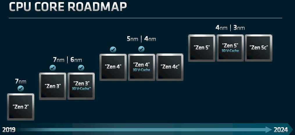
AMD has been pretty vague about what makes a Xen “c” core different from a regular core, but what we do know is that in the “Genoa” and “Bergamo” Zen 4 era, it allows for a cloud-optimized processor to have 128 cores with Bergamo coming in 2023 compared to the 96 cores in Genoa coming before the end of 2022. We have said for a long time that no all workloads need heavy floating point or matrix work, and thus ripping out vector units and now matrix units makes sense for these so you could cram more, skinnier integer cores onto a die. This is particularly true if these CPUs are going to be hooked to GPUs or FPGAs for acceleration – the vector and matrix units are superfluous on the CPU in this case.
What we infer from the chart above is that with the Genoa/Bergamo crank on the Epyc clock, the Genoa chip will be etched in 5 nanometers, with a plain vanilla version and a variant with 3D V-Cache, which boosts the performance and price/performance of certain HPC workloads by a lot. We happen to think that when the cost of 3D V-Cache manufacturing comes down, it should be standard because it inherently opens more die space to add more cores. But AMD is not taking this attitude, and we are trying to convince it otherwise, especially after reading a paper out of RIKEN Lab in Japan about how massive stacked L2 caches could drive performance of the A64FX processor by 10X by 2028. With Bergamo, it looks like AMD will shift to a refined 4 nanometer process from TSMC and rip some of the guts out of the Genoa to get more cores on the die. We think it will be a larger die, and possibly with its vectors gone. We shall see.
But as you can see, there will be this same distinction with the Zen 5 family of cores – two scoops of plain vanilla using 4 nanometer processes, two scoops of plain vanilla with 3D V-Cache on top using 3 nanometer processes, and three scoops of chocolate chip using 3 nanometer processes – used in the “Turin” family of processors coming in 2024. (We don’t have all of the code names, but there will be Turin, Turin-X, and something else from Italy, probably not “Pisa” because that is an engineering failure but public relations genius, you have to admit.)
Given the relative positions of AMD and Intel in PC and server CPUs these days, you can’t blame Papermaster for taking a bit of a victory lap for the Zen 3 core used in the “Milan” Epyc 7003 processors:
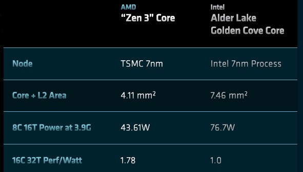
The “Golden Cove” core is used in the forthcoming “Sapphire Rapids” Xeon SP processor etched with Intel’s refined 10 nanometer SuperFIN process, known as Intel 7 now, so this Power-Performance-Area, or PPA, comparison is apt for the datacenter as well as for the desktop. Normalized for an 8-core, 16-thread chip running at 3.9 GHz, the Zen 3 core has 45 percent less area, burns 45 percent less power, and offers a smidgen more performance, which equates to a 78 percent better performance per watt. (AMD is mixing data for 8-core and 16-core chips in the chart above, which is annoying.)
The gap is going to get even wider with the Zen 4 core, apparently:
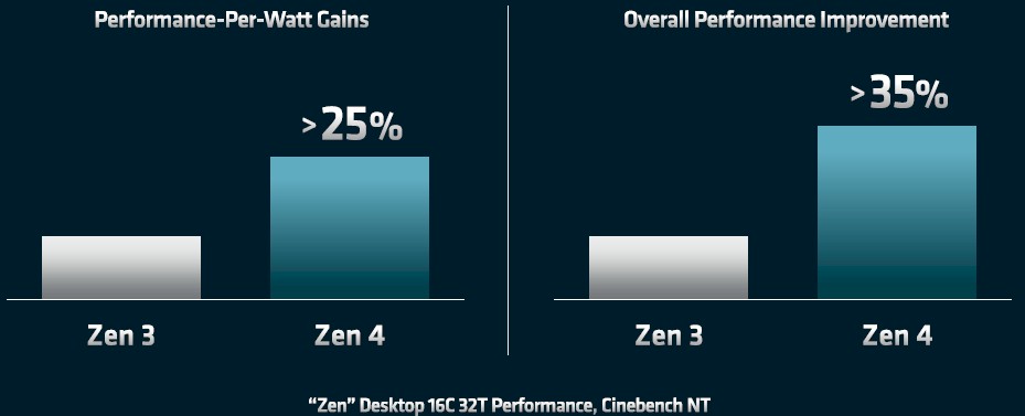
The initial Zen 4 cores used in the Genoa and presumably the Genoa-X processors are going to get an 8 percent to 10 percent increase in instructions per clock, and thanks to the move to the 5 nanometer processes at TSMC, will see a greater than 15 percent increasing in single-threaded performance, according to Papermaster. The Zen 4 cores will have support for AVX-512 vectors as well as “ISA extensions for AI,” which probably means a matrix math overlay for the AVX-512 math units, plus a 125 percent increase in memory bandwidth per core.
The net-net is that the Zen 4 core will have more than 35 percent more performance and more than 25 percent better performance per watt on a 16-core complex, which should mean Genoa has a 2.3X advantage on performance per watt on 16 cores compared to Sapphire Rapids at the same clock speed, and a slightly larger than 2X performance advantage on an 8-core complex at the same 3.9 GHz baseline. It also means that Genoa is running about 8 percent hotter than Milan if the power consumption and heat dissipation of the Epyc chips follows the same pattern as the desktop Ryzen chips that Papermaster used in his comparison. (Again, at constant clocks.)
Sapphire Rapids is not going to have a good day when Genoa launches; Intel really needs to get “Granite Rapids” into the field ASAP. So far, Intel has been one step behind AMD since the “Rome” Epyc 7002s were launched in 2019.
With Zen 5 cores, there is yet another “ground up” microarchitecture, which has a wider instruction issue and a new pipeline on the front end to make it more efficient and deliver higher performance. The Zen 5 core will also have optimizations for AI, as yet to be detailed, but it would not be surprising to see some of the AI Engines from the Xilinx Versal FPGA compute complexes, which are hard-coded arrays of DSPs for doing inference, added to the Epyc chips, much as IBM and Intel are adding matrix units to their respective “Cirrus” Power10 and “Sapphire Rapids” Xeon SP processors.
In his presentation, McNamara pulled out the Epyc server CPU roadmap, which obviously correlates to the Zen core roadmap that Papermaster showed. Take a look:
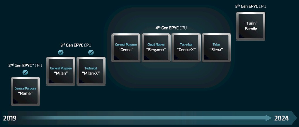
On these roadmaps, Zen 4 cores first appear in late 2022 in Genoa and then in Genoa-X, Bergamo, and now a new chip aimed at telcos and other service providers called “Siena” in 2023. The Turin family comes in 2024 with the Zen 5 cores, and McNamara said to expect the full complement of CPU types of general purpose, cloud native, technical, and telco. (There just wasn’t room on the roadmap to show them all.)
The Genoa chip, with 96 Zen 4 cores, will have 12 DDR5 memory channels and support for PCI-Express 5.0 peripherals and the CXL overlay for hooking accelerator memory to system memory over the PCI bus. The Genoa processor will have memory encryption on both DDR5 and any CXL-attached memory, and will have more than 75 percent higher performance on Java compared to the Milan Epyc 7003 with 64 cores. (That is 50 percent from more cores, 8 percent to 10 percent from higher IPC, and perhaps some clock speed boosts and other architectural changes to get the remaining 15 percent or more performance.)
The Bergamo Epyc 7004 variant with the Zen 4c cores comes in the first half of 2023 with 128 cores, which are ISA-compatible with the Zen 4 cores and have the same dozen memory channels and the same PCI-Express 5.0 (and presumably CXL) support. We had been wondering if AMD would remove simultaneous multithreading (SMT) to provide better security at the core and more deterministic performance (as Ampere Computing says it is delivering with its Altra Arm server CPU line), but McNamara’s presentation shows two threads per core, so scratch that. AMD will ship Genoa-X – the X is presumably for “extreme performance” but perhaps calling it Genoa-V would have been better so we can remember which one has the 3D V-Cache – sometime in 2023, but it is not saying when. Ditto for Siena, which is a Zen 4 CPU with up to 64 cores, but optimized to deliver the best performance per watt and the lowest cost as well as to be suitable for edge and telco uses. That sounds to use like it has some dud memory controllers and PCI-Express controllers and AMD is not letting these chips go to waste.
AMD spent a lot of time comparing the “Aldebaran” Instinct MI200 series to the Nvidia “Ampere” A100 GPU accelerator and didn’t mention the fact that its GPU rival Nvidia has unveiled the “Hopper” H100 kickers to it, which best the MI200s on some key metrics. We will get into fuller comparisons when the H100s ship, and are priced, later this year.
The interesting bit on the CDNA architecture for datacenter compute GPUs is the revelation that the Instinct MI300 is coming in 2023 and that it will be an accelerated computing unit, or APU, which is a device that combines a CPU and a GPU on a single device – like the one anticipated in 2017 but which never was launched. Here is the CDNA roadmap that shows the timing:
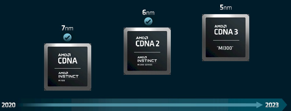
Here is the Instinct roadmap:
Admittedly, it doesn’t say much.
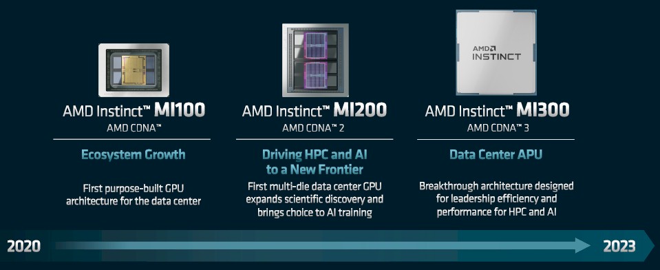
AMD has been dreaming about APUs since the peak days of the Opteron CPU way back in 2006, and it started rolling out its first APUs for PCs back in 2010. These were followed up by custom APUs in Sony PlayStation 4 and 5 and Microsoft Xbox XS series game consoles, and there were even a few Opteron APUs – the X2100 in 2013 and the X3000 in 2017. And while the AMD roadmaps call for aggressive evolution of its independent CPUs, GPUs, DPUs, and FPGAs, at least one variant of the future Instinct MI300 GPU will actually be an APU.
We have a hard time believing that there will not be a free-standing, four-GPU package in the MI300 series, for those customers who want a discrete CPU linked to a discrete GPU. The rumor has been that the MI300 would cram four GPU chiplets onto a single package, offering at least 2X more throughput than the MI250X at double precision floating point. But Wang did not talk about that in his GPU presentation. But he did talk about the CDNA 3 architecture and what we presume is the base for the Instinct MI300.
Here is the chart on the CDNA 3 architecture:
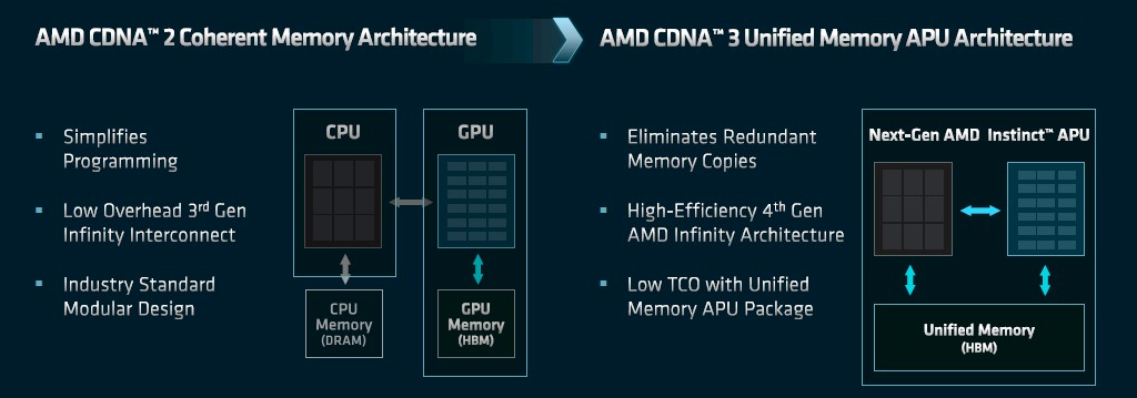
This is an important distinction that is made possible by creating an APU. With the combination of Epyc CPUs and Instinct GPUs today, the memory for these two devices is distinct and they are linked by Infinity Fabric 3.0 high speed links to each other so that the caches can cross connect and provide coherent memory access across those two devices. It’s like having a NUMA interconnect between CPUs, only it involves different kinds of memory and relatively high latency between the two devices. (It is still a lot less than reaching from a CPU to a GPU over the PCI-Express bus, though.)
With the CDNA 3 architecture, the CPU and GPU are chiplets implemented on the same package, linked to each other by Infinity 4.0 links, which have unified memory access. Meaning, either device can access the same memory on the device at the same time – with appropriate controls over which device is controlling the writing of data to memory, much as happens in NUMA devices. Importantly, there is no copying of data between the CPU and the GPU so they can do their work – they both to do their work in the same physical memory.
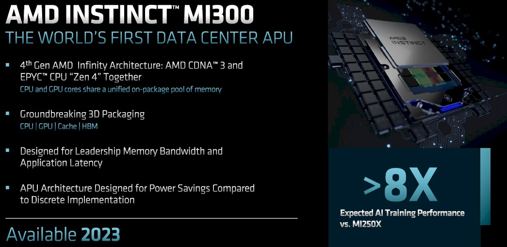
The feeds and speeds of the CDNA 3 GPU on the MI300 package were not revealed, but Wang said that the device would have more than 8X higher performance on AI training than the MI250X and offer more than 5X the “AI performance/watt,” whatever that means specifically. That could simply mean 2X the GPU cores plus a switch to FP4 floating point processing, which only works on certain kinds of AI training. (Nvidia has support for FP8 in the Hopper GPU, and so does Intel’s Gaudi2 custom matrix math ASIC for AI training. No one has FP4 as yet, but it would not surprise us when it does become available.) The Instinct MI300 package has Epyc 7004 chiplets with the Zen 4 cores as well, and it looks like both the CPU and the GPU will be sitting atop an Infinity Cache L3 cache memory, which has been used in the Radeon Pro RDNA 2 graphics GPUs already. The MI300 chiplets will be etched in TSMC 5 nanometer processes and make use of 3D packaging techniques. The 2.5D Elevated Fanout Bridge interconnect that was used in the Aldebaran GPUs to link these compute engines to HBM memory will presumably be used to link the CPUs and the GPUs to HBM3 memory on the package; it is not clear that the 3D hybrid bonding technique used in the Milan-X server CPU to triple its L3 cache (3D V Cache) is being used for the Infinity Cache.
As we said above: Not everyone is going to want a static ratio of CPU to GPU compute, so we have to believe that there will be an Instinct MI350 and MI350X, possibly with a lot more GPU chiplets on them but based on the AI training ratios, it looks like AMD might be getting four GPUs on a package with 64 CPU cores. That would basically be a node of the “Frontier” supercomputer on a single package – no mean feat if it turns out to be true, and probably hot enough to cook hamburgers and hot dogs on.
That leaves the FPGA and AI Engine compute fabrics from Xilinx and the embedded product lines, which are important for edge, industrial, and other use cases where the compute needs are different than in the core datacenter. Here is the roadmap that Peng revealed for the two businesses he now runs at AMD:
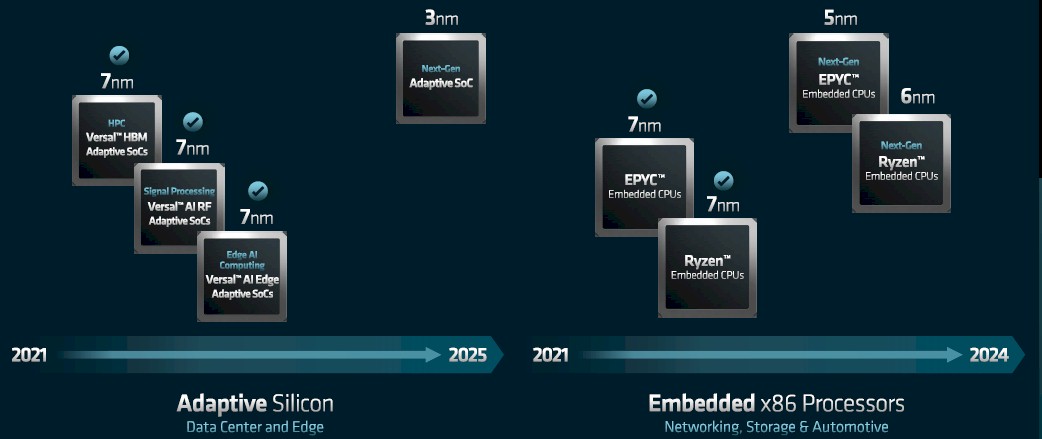
The interesting bit here is that AMD is skipping the 5 nanometer node in 2024 with the Versal FPGA kickers, which were not expected to launch this year anyway since they are still ramping production on many Versal SKUs. So of course it is moving to 3 nanometer processes at TSMC for the Versal kickers in 2025. And that will be a phased rollout as was the case with the “Everest” Versal devices, which were revealed way back in October 2018 and which still have several more years of life in them. (Given the nature of the customers and the programmability of FPGAs, they don’t have to be on the same rapid cadence as CPUs, and take even longer than a new generation of GPUs to come to market.)
AMD and Xilinx have not talked much about how Xilinx technology would be integrated with AMD technology, which we speculated upon back in February as the deal was closing. We do know the plan is to being the AI Engines to the Ryzen client CPUs to speed up inference and we now know that the Epyc family will eventually get some bits of Xilinx “XDNA architecture” sprinkled upon them. Take a look:

We would love to find out how programmable logic might be added to Epyc CPUs as well as the hard-coded AI Engines DSP engines for matrix math. And we would also love to know how companies are supposed to figure out when they might need co-packaged chiplet engines of various architectures and when discrete CPUs, GPUs, FPGAs, and AI Engines are suitable. And why not just an AI Engine accelerator all by itself, without any FPGA programmable fabric, as a discrete device? If you want to give customers all of the options, then make all of the options.
By the same logic, there should be FPGAs that don’t have Arm cores – or indeed any cores – on them, just a programmable logic block that can be linked to CPUs and GPUs over Infinity Fabric links and, later, Infinity Fabric links sporting the Universal Chiplet Interconnect (UCI-Express) protocol that Intel is trying to make a standard inside of the package like it has with CXL across distinct memories on CPUs and accelerators.
Next up, we will take a look at the unified AMD-Xilinx software stack that is coming together and also review what the company said about its aspirations in datacenter networking.

AMD Is Finally Trusted In The Datacenter Again
This is how a competitive chip market is supposed to look, and this is how a competitive chip maker recovers from faults, competes against a seemingly unassailable foe, and then rides up the revenue and income curves to be able to invest in the future and profit from the present. …
AMD Rounds Out “Aldebaran” GPU Lineup With Instinct MI210
When the “Aldebaran” datacenter GPUs were launched by AMD last November for the HPC and AI crowd pushing up into the exascale stratosphere, only the two top-end models of the Instinct GPU accelerators –ones that use the Open Accelerator Module (OAM) form factor put forth by Facebook and Microsoft under …
Intel Unfolds Xeon Roadmap With More Cores, Denser Transistors
We were complaining a few weeks ago that Intel had not put out a server processor roadmap of any substance in a long time, and instead of just leaving it at that, we created our own Xeon SP roadmap based on rumors, speculation, hunches, and desires. In the absence of …
“The initial Zen 4 cores used in the Genoa and presumably the Genoa-X processors are going to get an 8 percent to 10 percent increase in instructions per clock, and thanks to the move to the 5 nanometer processes at TSMC, will see a 15 percent increasing in single-threaded performance, according to Papermaster.”
Look at the Slide at AMD Finical Analysts Day and you will see that “>” symbol in front of the 15% so that reads Greater Than 15%. But If AMD does not dust of its Project K12 Custom ARM core that Jim Keller/K12 Team designed then expect that AMD will get pushed out after a while from the Handheld Gaming Devices market by Qualcomm and it’s Nuvia Custom ARM core engineers and Nuvia was founded by former Apple A/M series SOC engineers so AMD better have retained the Verilog for K12 and be preparing for the Future of the handheld gaming market where AMD currently has sold a lot of x86 based APUs. But watch out for ARM there on the higher end from Qualcomm if in fact they can field a very wide order superscalar custom ARM core similar to Apple’s A14/Firestorm core and Nuvia’s engineers have some experience there in that process. And ARM in the server market is not slowing down so AMD had better give up on any x86 duopoly fixation and get back to development for ARM, or even RISC-V, and as for handheld gaming ARM processors have the better battery life and even if AMD’s got some market for x86 there AMD needs to thank the Gods that Apple has not launched a handheld Like the Steam Deck with Apple’s A14, or A15, processor inside. Watch out for Qualcomm in the Laptop space and ARM based processors there sometime in 2023/later time frame!
Yup on the greater sign. Thanks for the catch.
“Next up, we will take a look at the unified AMD-Xilinx software stack that is coming together and also review what the company said about its aspirations in datacenter networking.”
Haven’t noticed this article yet, is it up on the site?
Yup. Here it is:
https://www.nextplatform.com/2022/07/08/now-comes-the-hard-part-amd-software/