It is a relatively quiet International Supercomputing conference on the hardware front, with no new processors or switch ASICs being announced from the usual suspects. While Trish Damkroger, general manager of Intel’s high performance computing division, gave the keynote opening up ISC 2021, providing a little more insight into the “Sapphire Rapids” Xeon SP processor and “Ponte Vecchio” GPU accelerator now due next year, starting with the “Aurora” A21 exascale supercomputer at Argonne National Laboratory, most of the feeds and speeds of these chips remain a mystery.
No one has officially said that the Aurora machine has slipped from its revised delivery date of the end of 2021, but that has been the suspicion since Intel announced a slip in its 7 nanometer process, which is used to etch parts of the Ponte Vecchio GPU, also known as the Xe HPC device, last July.
At that time, the plan had been to have Aurora in the field at Argonne by the end of 2021, but this seemed unlikely given that then-CEO Bob Swan told Wall Street that initial shipments of Ponte Vecchio would slip to late 2021 to early 2022. Intel revised the Ponte Vecchio plan to use a mix of chiplets etched in its own foundries as well as those of its competitors, in this case Taiwan Semiconductor Manufacturing Corp, which actually has a working 7 nanometer process unlike Intel and GlobalFoundries. (Samsung, the only other 7 nanometer chip supplier and IBM’s partner for Power10, is working on it.)
Damkroger did not mention, by the way, that Intel is actually pushing out the delivery date for the Sapphire Rapids Xeon SP processor, which is being etched using the Enhanced SuperFin tweak of Intel’s 10 nanometer manufacturing process. But Lisa Spelman, general manager of the Xeon and Memory Group in the recently reorganized Intel, did put out a blog post explaining the delay in shipping the server chip at the heart of – well, more like the medulla oblongata of since the Ponte Vecchio GPUs do most of the thinking – the Aurora system. Now both Sapphire Rapids and Ponte Vecchio have slipped and it seems highly unlikely that Argonne will get the core parts of the system this year.
In any event, the Sapphire Rapids slippage affects more customers than the Ponte Vecchio slippage does, and now it looks like Ponte Vecchio will beat Sapphire Rapids into the field.
The Sapphire Rapids chip is based on the “Golden Cove” core, which has a new microarchitecture that includes two new accelerators that Spelman talked about. The first is called Advanced Matrix Extensions, or AMX, and we suspect that it is a matrix math overlay on top of the AVX-512 vector engines that pumps up the performance of matrix operations akin to that done by Tensor Core units on Nvidia GPUs as well as matrix overlays for vectors in IBM’s future Power10 chips. Spelman is not spilling the beans on AMX, but says that on early silicon for Sapphire Rapids, machine learning inference and training workloads are running 2X faster than on the current “Ice Lake” Xeon SP processors, which merely sport mixed precision in their vector engines to boost AI throughput.
Another forthcoming feature in the Golden Cove core – at least the variant aimed at servers – is called Data Streaming Accelerator, or DSA, and it was designed for various kinds of high performance workloads to boost the performance of streaming data movement as well as the transformations operations that are often done to streaming data in storage, networking, and analytics workloads.
“Demand for Sapphire Rapids continues to grow as customers learn more about the benefits of the platform,” Spelman said in a blog announcement. “Given the breadth of enhancements in Sapphire Rapids, we are incorporating additional validation time prior to the production release, which will streamline the deployment process for our customers and partners. Based on this, we now expect Sapphire Rapids to be in production in the first quarter of 2022, with ramp beginning in the second quarter of 2022.”
People at AMD must be giggling and snickering. Probably those at Ampere Computing, too. We can hear the “Sapphire Not So Rapids” and a “Ponte Vecchio Too Far” jokes from afar. . . .
It is hard to say when the successor to the current “Ice Lake” Xeon SP was due to come to market because Ice Lake itself bopped around so much. Ice Lake was delayed about three years when it launched in March, so that should have put what became Sapphire Rapids somewhere 18 to 24 months after that. Call it March 2019 to be generous. What this now means is that the 10 nanometer chips are still running three years behind after this delay and have not been able to catch up. Hopefully for Intel’s sake, there won’t be another delay with the “Granite Rapids” Xeon SP that will be etched with 7 nanometer processes. After the July 2020 delay, the Granite Rapids Xeon SP processors slipped to the first half of 2023 compared to the expected launch in early to middle 2022. Which is when Sapphire Rapids is now hitting.
The big reveal at ISC 2021 was that there will be a variant of the Sapphire Rapids processor aimed at HPC and AI workloads that will include HBM memory. “Sapphire Rapids will be out before Sapphire Rapids with HBM, but roughly in the same timeframe,” says Damkroger. “And anybody will be able to buy Sapphire Rapids with HBM. You can use the HBM alone, or you can use it with DRAM.” This is an interesting development indeed. And as Damkroger said, this will not just be a special SKU that only select customers can buy. The question is, what will the HBM addition cost, and how much performance will it add.
There are some rumors running around about what Sapphire Rapids with HBM will look like, one of which you can see here and which seems pretty plausible. This report says that the Sapphire Rapids chip has four 15-core tiles for compute, with one core inactivated, presumably to drive up effective yield. So the maximum core count per socket is going to be four times fourteen or 56 cores, with a possible leap to 60 cores if the 7 nanometer yields get good.
This approach is exactly what IBM is doing with its Power10 chip, which has 16 physical cores and only 15 cores are being activated from the get-go because they know yields on Samsung’s 7 nanometer process will be – how should we put this? – troublesome. And before you start, remember that with the “Pascal” and “Ampere” GPU designs, Nvidia did the same thing with TSMC’s 7 nanometer processes.
It is not clear if these Sapphire Rapids sockets are made of chiplets, which would mean having I/O and memory controllers separated from core blocks, or if they are whole CPUs that are implemented in multichip fashion, as AMD did with the “Naples” Epyc 7001s and earlier Opterons a long time ago and as IBM has been doing since the Power5 in 2005. There are four HBM2 stacks, so they could all have their own memory and it can be an MCM, if this report is correct. The HBM2 stacks are four high with 16 GB of capacity, for a total of 64 GB per socket. And that is a perfectly reasonable amount of main memory for an HPC and AI application, and with a 1 TB/sec bandwidth, that is also pretty reasonable. The HBM capacity could be doubled, we think, to 128 GB pretty easily but not cheaply, with an eight-high stack. It is not clear how much DDR5 memory this Sapphire Rapids socket will address, but it is likely going to be at least 512 GB and probably 1 TB and maybe even 2 TB.
The top end Sapphire Rapids chips are expected to weigh in at 400 watts, including their HBM2 memory. We joked a long time ago that all computing would look like graphics cards in the long run. This has certainly held true for the Fujitsu A64FX and the NEC Aurora processors used in HPC (that’s a different Aurora), and in the long run you can expect an HBM variant of Epyc as well. That, in fact, might be one of the secrets in the exascale systems that the Cray unit of Hewlett Packard Enterprise is building for the US Department of Energy.
We already know that Intel and HPE/Cray are using a two-socket Sapphire Rapids node with six Ponte Vecchio GPU accelerators linked over the PCI-Express 5.0 bus using the CXL 1.1 protocol to the CPUs. Three GPUs per CPU, just like in the “Summit” supercomputer at Oak Ridge National Laboratory built by IBM and Nvidia.
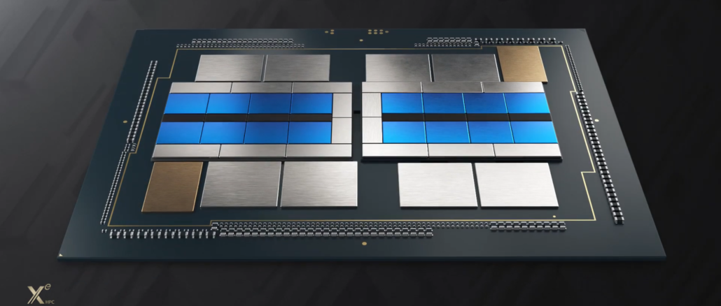
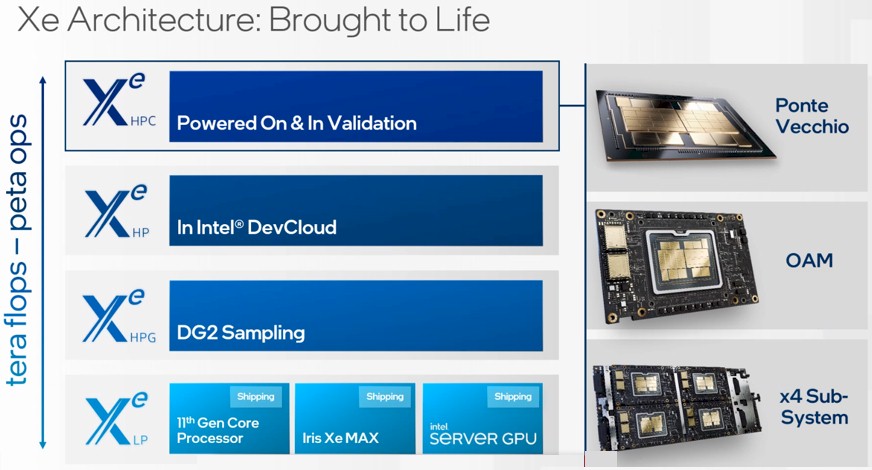
The Ponte Vecchio Xe HPC GPU accelerator, shown in the feature image at the top of this story, has 49 tiles and over 100 billion transistors. It is a beast, and it has been powered on and early silicon is going through testing and validation, according to Damkroger, and she also mentioned the other form factors that will be available, as you can see above. There is a four GPU subsystem as shown, based on the Open Compute Project’s Open Accelerator Module, as well as an eight GPU subsystem not shown, which presumably also hews to the OAM specification. Presumably these will have coherent interfaces over CXL between the GPUs and out to the CPUs using a PCI-Express 5.0 switch fabric.





“Intel revised the Ponte Vecchio plan to use a mix of chiplets etched in its own foundries as well as those of its competitors”
Raja stated that Ponte Vecchio was designed from the start to use a mix of chiplets from internal and external foundries.
I think Intel has said it was designed so it
could
do it, but I do not believe the plan from the beginning was that it
would
do it.
O monstro tá saindo da jaula… Exaflop boyyy…