
If you had to sum up the second half of 2022 and the first half of 2023 from the perspective of the semiconductor industry, it would be that we made too many CPUs for PCs, smartphones, and servers and we didn’t make enough GPUs for the datacenter. Or rather, Taiwan Semiconductor Manufacturing Co, the world’s largest and most important chip foundry, didn’t.
The world would probably buy somewhere between 1 million and 2 million datacenter GPUs this year, but apparently Nvidia could only make on the order of 500,000 of its most advanced “Hopper” H100 devices this year, and that was limited by the availability of the Chip on Wafer on Substrate (CoWoS) 2.5D packaging technique that has been in use along with HBM stacked memory for GPUs and other kinds of compute for the past decade.
And so, TSMC has had to make the best of the situation even as revenues and earnings remain in a slump and the cost of each successive manufacturing process node gets more and more expensive.
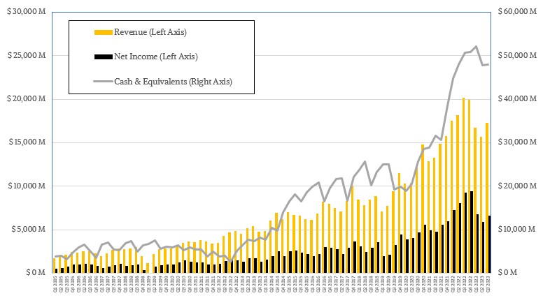
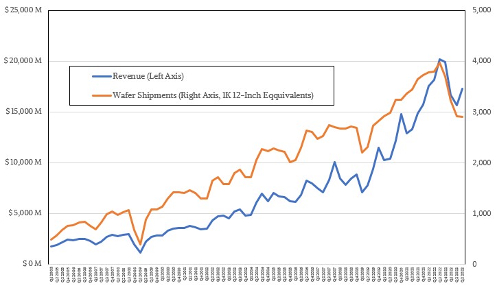
In the third quarter ended in September, TSMC’s revenues were down 14.6 percent to $17.28 billion and net income fell by 28.1 percent to $6.66 billion. The various IT channels are still burning off their capacity of CPUs and GPUs for client devices, and the hyperscalers and cloud builders are also digesting the tens of billions of dollars in servers and storage that they acquired in 2022 and only buying what they need now as they await the next generation of devices and another heavy investment cycle that could start next year.
Everyone is shifting some of their server, storage, and switching budgets in the datacenter to higher cost and more strategically important AI training and inference systems as the generative AI boom is well underway – and there is no sign of that boom stopping anytime soon after a period of hyperinflation this year. And so, GPUs and anything that can do matrix math like a GPU are almost worth their weight in gold as companies try to figure out how to weave generative AI capabilities into their applications during a period of intense demand and limited supply.
In these cases, TSMC can charge more for its advanced chip etching and packaging capacity, but not enough to offset the declines in other parts of its business. Unlike, say, Nvidia, which can pretty much charge whatever it wants for any GPU that it can get out of the factories. Its financials will continue to defy gravity for a while. But eventually, as capacity constraints ease supply will catch up with demand and prices will normalize. But not this year, not even as Nvidia doubles its CoWoS capacity and seeks to increase it further through 2024.
TSMC has to cope with a lot of tensions in its line of work, and one of them is that it has to do a lot of research, development, and capital investment to make sure it can keep advancing the state of the art in semiconductors. And when business slows, as it has in recent quarters for reasons sometimes out of its control and sometimes because it is difficult to plan for booms like the one that took off for GenAI in late 2022, the company has to make a lot of calls about when to curtail capital spending and still not leave itself flatfooted. That’s because TSMC’s customers can benefit much more from supply shortages and high demand than it can. Again, Nvidia is the illustrative case in point.
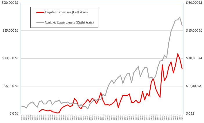
In the September quarter, TSMC really pulled back on the capital investment reins, spending only $7.1 billion, a decrease of 18.9 percent compared to the year ago period and also representing a 13.1 percent sequential increase from the $8.17 billion the company spent on factories, etching equipment, and so forth in Q2 2023. Wendell Huang, chief financial officer at TSMC, said on a call with Wall Street analysts that TSMC was expecting to spend only $32 billion for capital expenses in all of 2023, with 70 percent being for advanced chip making gear at the smallest nodes (5 nanometers and lower these days), 20 percent for specialty technologies that tend to be at larger nodes (12 nanometers up to 28 nanometers), and about 10 percent on packaging, testing, and mask making gear. That means capital expenses in Q4 2023 will be around $6.8 billion, a drop of 32.7 percent.
This is as the ramp for 3 nanometer processes is well under way and 2 nanometer technologies are building momentum towards ramp.
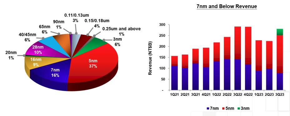
The third quarter was the first where TSMC sold products based on 3 nanometer processes, and this node already accounted for 6 percent of revenues, or just over $1 billion out of the chute. Chips etched with 5 nanometer processes drove $6.39 billion in revenues, or 37 percent of the total, while 7 nanometer processes still drive 16 percent of revenues, or $2.76 billion. All other processes, ranging from 12 nanometers all the way up to 250 nanometers drove the remaining $7.08 billion in sales. All of those older nodes have plenty of use – a lesson that Intel forgot because it was a foundry with only one customer, and one that always needed to be at the bleeding edge to compete in CPUs.
“N3 is already in volume production with good yield and we are seeing a strong ramp in the second half of this year, supported by both HPC and smartphone applications,” explained CC Wei, chief executive officer at TSMC, on the call. “We reaffirm N3 will contribute mid-single-digit percentage of our total wafer revenue in 2023, and we expect a much higher percentage in 2024 supported by robust demand from multiple customers.”
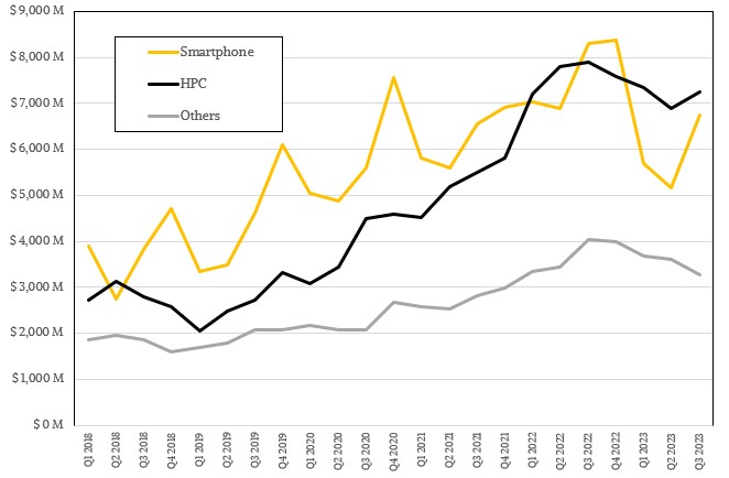
Remember that when TSMC says “HPC” it means any kind of high performance silicon, which can be a PC or server CPU or GPU or a networking ASIC. TSMC does not mean ASICs dedicated to HPC simulation and modeling or AI training or inference – although these certainly are within the scope of TSMC’s HPC definition. The 3 nanometer node will be a long-lasting one, with an N3E crank having just passed qualification further enhancements in the N3P and N3X processes in the works. The N5 node has been in production since Q3 2020, just to give you a sense of how long these nodes can be in the field, and it has only just become the dominant revenue generator. The N7 nodes are on the wane, of course, but will also be in the portfolio for a long, long time.
Like Intel 18A, TSMC N2 will employ a nanosheet transistor structure and will drive both transistor density and power efficiency. For smartphone and HPC applications, which drive the business, Wei said that interest in N2 is at or higher than it has been for N3 at the same point in their development and production cycles. The backside power rail adjunct technology for N2 will be available in the second half of 2025 and put into production in 2026.
As for who will have the lead in process in 2025, Wei is having none of the smack talk of Intel 18A versus TSMC N2.
“We do not underestimate any of our competitors or take them lightly,” Wei said. “Having said that, our internal assessment shows that our N3P – now I repeat again, our N3P technology – demonstrates comparable PPA to 18A, my competitor’s technology, but with an earlier time to market, better technology maturity, and much better cost. In fact – let me repeat again – our 2 nanometer technology without backside power is more advanced than both N3P and 18A and will be semiconductor industry’s most advanced technology when it is introduced in 2025.”
Your move, Pat.
Last thing. TSMC did not divulge how much of its revenues were being driven by AI training and inference workloads, as it did during its Q2 2023 conference call. But if the ratio between AI revenues and TSMC HPC revenues is consistent, then it should have been just shy of $1 billion. That seems low to us, but it might just be an indication of how much profits companies like Nvidia and AMD can extract from GPU sales these days.
If you can make a compute engine for an Nvidia or an AMD a few hundred bucks and add HBM memory for a few thousand bucks and then an Nvidia or an AMD can sell the complete device $30,000 and then maybe get another 2X factor in sales turning those compute engines into a system with lots of CPU compute, CPU memory, flash storage, and networking, this becomes a very big business. So that $1 billion in AI training and inference chip sales for TSMC can balloon up to tens of billions of dollars in hardware spending at the end user level – even if those end users are hyperscalers and cloud builders among the Super 8 or Top 10 or whatever who get steep volume discounts from companies like Nvidia and AMD.
Maybe TSMC and its downstream chip partners and further downstream partners could adopt a new short-term strategy: The more you buy, the even more you should pay. At this point, it is just as logical to say that those who need 20,000 GPUs should pay more per unit than someone who needs only 200 or even 2,000 as it is “logical” to say they should be paying less, as the IT market seems to have believed for decades.
Right?

The Big Clouds Get First Dibs On AMD “Genoa” Chips
The expanded lineup of AMD’s 4th generation “Genoa” Epyc server chips – built atop “Zen 4” core and some with the chip maker’s L3-boosting 3D V-Cache – unveiled at a high-profile event in San Francisco this week is quickly making its way into the cloud. Microsoft and Amazon Web Services both …
Intel And AMD Make X Less Of A Variable For X86 Processors
One of the oldest ideas in humanity – and one that may have predated language as we know it – is that the enemy of my enemy is my friend. Another adage is that he who has the gold makes the rules, and in the datacenter market these days, the …
Intel Tests Its Datacenter Teflon With 7 Nanometer Delay
There is such a thing as a string of bad luck, but we have always believed that luck is the residue of design, either good or bad. And so it is hard not to lift a skeptical eyebrow pretty high, given the many-year delay in the rollout of 10 nanometer …
Good to see TSMC coming out of that Q2 “What The Heck???” trough (TNP 07/21/23) with most indicators now nicely up! Hopefully they make that 3,500 1K-12″-eqs wafer shipments foretold by 8^q (unusual name)’s non-AI crystal ball incantations by the Q4 report in Jan ’24 (if only to demonstrate the awesome power of the non-AI metaphysical mind! eh-eh-eh).
“All of those older nodes have plenty of use – a lesson that Intel forgot…”
Intel’s recent chips are using tiles built on different processes… some tiles on TSM EUV and some on Intel DUV. Their base tile on Meteor Lake is reported to be 22FFL.
These have been in design for a few years, so it isn’t like they just remembered…