

We are not shy of playing guessing games here at The Next Platform, as you all well know. And Intel and Cray have left us with a few big ones with regard to its future “Aurora A21” exascale system that Intel is the prime contractor for and Cray is the manufacturing subcontractor for at Argonne National Laboratory. But some of the pieces of the puzzle are falling into place at the SC19 supercomputer conference in Denver.
The A21 details got us to thinking as well about the feeds and speeds of the future 1.5 exaflops “Frontier” supercomputer coming to Oak Ridge National Laboratory in 2022. We have some thoughts on that machine, too.
Let’s talk a bit about the A21 system at Argonne first.
As part of its adjunct HPC DevCon event ahead of the SC19 show and some revelations about its future Xe line of GPUs and the discrete accelerators based on them, Intel divulged some basic information about the hybrid CPU-GPU node that will comprise the updated Aurora machine. It is significantly different from what Intel had proposed for the original pre-exascale Aurora system, which was supposed to replace the big BlueGene/Q system at Argonne with a cluster with more than 50,000 nodes and somewhere around 180 petaflops initially using the now equally defunct “Knights Hill” Xeon Phi processors and 200 Gb/sec Omni-Path interconnect. Intel formally discontinued these during 2019, but they were practically dead products about a year before that.
The original 180 petaflops Aurora was expected to cost around $200 million; that node count was very high and the average peak performance per node was only around 3.5 teraflops – not much more than what the 72-core “Knights Landing” Xeon Phi processor announced in 2015 and delivered in 2016 provided. Our presumption – and based on some pretty good guesses that in turn were based on a presentation that Intel chief HPC architect Al Gara gave in 2015 that the whole point of Knights Hill – was to break up the Knights processor into smaller chunks and shift entirely from a mix of far DRAM and near MCDRAM to a bigger chunk of stacked HBM2 memory like video cards and other accelerators used. The idea was to get the processor yields up, the costs down, and the ratio of compute to memory bandwidth back into alignment and memory capacity to compute capacity in better alignment by using a mix of HBM2 and Optane memory throughout the system. Everything had to be changed because of AI workloads converging with HPC workloads. Whatever Knights Hill was, it apparently was not going to be as good as a GPU at AI workloads, and maybe even not HPC applications that had been accelerated already on Nvidia GPUs with its CUDA environment.
As we reported back in March, the revised Aurora contract came in at a considerably higher figure. Intel, the prime contractor, will get over $500 million, with Cray receiving more than $100 million of that for its Slingshot interconnect, the more than 200 Shasta cabinets that will comprise the system, and the Linux software environment that will glue it all together. Intel is also kicking in some of the software stack, and it is not clear where the lines between Intel and Cray code will be drawn. Intel gets the rest to cover the cost of processors, main memory, Optane persistent memory, and other aspects of the system. Aurora is anticipated to be delivered in 2021, with acceptance by Argonne expected in 2022.
The expectation is that this will be the world’s first exascale system, but we are hearing chatter that it will not be. People in the know won’t tell The Next Platform who is rumored to be the frontrunner in the global exascale race. We though it might be the “Fugaku” system at the RIKEN Center for Computational Science in Japan, but have subsequently learned that Fugaku will top out at 150,000 nodes and 400 petaflops at double precision floating point. There is always an outside chance that China will get one of its three known exascale systems to market next year, too. Frontier could beat out Aurora A21. No matter what, you can bet one thing for sure, and that is that the United States, China, and Japan all want to be first to reach this important milestone. Take this with a grain of salt.
The other rumor we hear, and which Intel and Cray are certainly not going to confirm, is that Aurora A21 will weigh in at 1.3 exaflops peak at double precision floating point, not the 1.1 exaflops many had been expecting. At this peak double precision performance and the expected computational efficiency, the A21 machine should yield a little north of 1 exaflops on the High Performance Linpack benchmark test that is used to rank supercomputers and other distributed systems that have no business being on the Top 500 list because they do not do HPC or AI as their day jobs.
After Intel’s disclosures this week, we know a little bit more about the basic shape of the A21 nodes. Take a look:

This is very interesting indeed. The A21 node will be configured similarly to the nodes used in the “Summit” supercomputer at Oak Ridge National Laboratory, and built by IBM with the help of Nvidia and Mellanox Technology. But it will be globally replacing the pair of “Nimbus” Power9 processors with future “Sapphire Rapids” Xeon SP processors, etched in the third generation of 10 nanometer processes from Intel’s foundries, and globally replacing the six Nvidia “Volta” Tesla V100 accelerators with the “Ponte Vecchio” Xe discrete GPU accelerators that we told you about earlier this week.
Let’s pick apart these CPUs and GPUs used in the A21 nodes, starting with the CPUs and their current roadmap:

Last December, Intel talked about the new “Sunny Cove” core design that will be implemented in the forthcoming and much delayed “Ice Lake” Xeon SP processors. The Sapphire Rapids chips will be using a much-improved core, and based on the timing in the roadmap presented last year, we think it will be the “Golden Cove” core, but it could be the “Willow Cove” core. Take a gander at that core design roadmap here, which shows the core names for the Core (meaning the client chip subset of the Xeon server chips) and Atom lines:
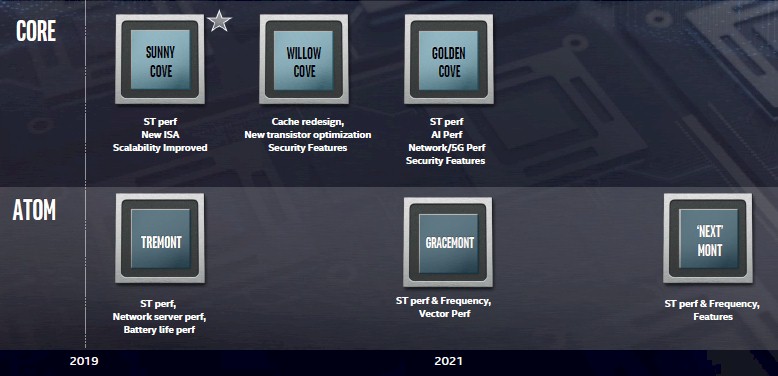
It is hard to say exactly what Sapphire Rapids will look like, but it is safe to say based on the roadmap above and others we have seen that the cores used in this server chip will have one or two bumps of single-threaded integer performance and that its AI performance, which means inference, will be goosed as well, probably with finer-grained mixed precision on its vector units and quite possibly for both integer and floating point data formats. Sapphire Rapids will certainly include the new instruction set that comes with Sunny Cove cores and employed the Ice Lake Xeon SPs, plus the cache redesign and optimizations of the Willow Cove cores, and probably the single threaded performance bump in the Golden Cove cores.
The question is how many cores will Intel deploy. Well, Intel has presumably shifted to a chiplet architecture started with the Ice Lake Xeons, and if it hasn’t then it is being really silly. It needs to do a total of 64 cores per socket to compete with AMD’s “Rome” Epyc 7002 series chips, and it if hasn’t done that, it is being doubly silly. The question is how far can Intel push it with the Sapphire Rapids package? Can it do 50 percent more cores, or can it get by with the same number of cores and just do an architectural enhancement on the cores? The answer is yes, it can do that, because that is precisely what AMD is going to be doing with the Zen 3 cores in the third generation “Milan” Epyc 7003 processors due in 2020. Intel can’t beat AMD to market with improved cores, but it can stall AMD some with its Xeon roadmap, promises parity in the not-too-distant future after Milan is announced. Intel may have no other choice.
The Ice Lake Core client chip has four cores and a big integrated GPU on it. It would be convenient if the server chiplet and the client chiplets were the same and the GPU was just done on package, and let’s therefore assume that Intel has cooked up bigger chiplets with more cores for the Ice Lake Xeon SPs. AMD has eight chiplets with eight cores each, and that seems to strike the balance between client and server needs, so why wouldn’t Intel do the same. It also stands to reason that Intel would not want to change the chiplet architecture too much from Ice Lake to Sapphire Rapids, much as AMD is not doing between Rome and Milan.
So, if you put a gun to our heads, we would say the A21 nodes will have two Sapphire Rapids Xeon SP processors, each with 64 cores per socket. There is an outside chance Intel could boost that to maybe 72 cores if it is feeling the heat from AMD’s Milan, but that would either mean using a different chiplet size or chiplet count from than Ice Lake. We think Intel would increase the chiplet count and take the NUMA hit. And it better have a central I/O and memory hub like AMD has in the Rome and Milan chips, now that we think of it.
The CPU does not matter all that much, but remember, Argonne has lots of codes that were originally running on CPU-only BlueGene/Q machines and CPU-only Knights Landing machines. So it still matters for many applications.
That takes us to the Xe GPUs. We know it is going to have lots of matrix math vector engines as well as lots of double precision floating point. People have been hinting to us that it will have some other features and functions that no one else is expecting, and we think there is an outside chance that Intel will embed a small version of its Configurable Spatial Accelerator (CSA) architecture on the device, or maybe better still, provide that dense matrix compute using CSA units. We Talked about the CSA architecture back in August 2018 based on an Intel patent filing, and there is nothing consistent with what the CSA is doing and creating a GPU with lots of integer and floating point units. For all we know, the integer and floating point units will use this CSA architecture and the matrix math vector units we expect on the Xe GPUs will be an Intel riff on Nvidia’s Tensor Core. If you can make the CSA behave like a block of integer and floating point units a GPU needs for graphics or compute and then change it to be a dataflow engine on the fly to directly process graphs, that would be really cool.
All we can really get a bead on with something that has error bars that are not too large is the double precision floating point power you might expect from the Sapphire Rapids Xeon SPs and the Xe GPU accelerators.
Intel has confirmed that the A21 machine will have more than 200 cabinets of compute, and it is hedging on how much compute that might be and if that includes storage as well as compute nodes. Each “Shasta” cabinet using the water-cooled, custom-sized racks can house 256 two-socket Rome Epyc nodes per cabinet in an all-CPU configuration, and in this setup, that Rome blade has four two-socket nodes per blade. So that is 64 blades per chassis. We know from the picture above that each A21 blade will have two Xeon SPs and six Xe GPUs per blade, and that works out to 128 CPUs and 384 GPUs per cabinet. If you look at 200 cabinets of this, that is 12,800 nodes. If you assume that 98 percent of the compute is in the GPUs, which is a reasonable assumption based on real-world clusters like those at Italian energy giant Eni, then at 1.26 exaflops double precision for 76,800 GPUs, that works out to 16.4 teraflops per Xe GPU. That’s only 2.2X the amount of FP64 performance compared to the current Tesla V100 GPU.
If that is too much of a performance leap to expect from the Intel discrete Xe GPU – and we think it is – Intel could just add cabinets. So, with a GPU that matches the 64-bit floating point performance of the current Volta GPU from Nvidia, it would take 438 Shasta cabinets to reach 1.3 exaflops peak at double precision. We think that if Nvidia did a process shrink from the 12 nanometers used with Volta to 7 nanometers at Taiwan Semiconductor Manufacturing Corp, it might be able to add just under 2X the number of CUDA and Tensor Core units to the device across a wider array of SMX units. Let’s call it around 1.65X for arguments sake. That 250 cabinet number is where a machine using an improved Nvidia Volta or an Intel Xe as the GPUs has the same number of GPUs and reaches the same 12.5 teraflops of peak FP64 performance. This all assumes that the Sapphire Rapids CPU has about 3 teraflops of performance of its own at double precision, and that 92.5 percent of the peak FP64 compute is in the GPUs.
We don’t know if we should call that improved Volta by the “Ampere” codename or not. But clearly Intel and Nvidia have done the same math as outlined above, and they are trying to beat these scenarios as best they can.
Clearly, AMD has done the same math for its future CPUs and GPUs, and a year later, we will see a hybrid node in the 1.5 exaflops “Frontier” system at Oak Ridge National Laboratory using a custom Epyc processor (a modified “Genoa” generation, we think) coupled to four custom Radeon Instinct GPU accelerators as the basic node in that machine. Let’s assume that the modified Genoa Epyc chip comes in at around 3.5 teraflops of its own FP64 peak performance. Then working backwards, we can pull out the aggregate FP64 compute across 200 Frontier cabinets, which works out to 90 petaflops across 25,600 of those Epyc chips and 1.41 exaflops across those 102,400 Radeon Instinct GPUs for 13.8 teraflops per GPU. The GPUs represent 94 percent of peak FP64 capacity. These numbers don’t violate our sensibilities. The AMD GPUs coming out a year later than Intel’s have 9.9 percent more FP64 oomph, and the AMD CPUs coming out a year later have 15 percent more. Nothing crazy.
At 200 cabinets, with two of those 1×4 AMD nodes in each sled in the Shasta machine, or at 100 cabinets with four of those 1×4 nodes, this is admittedly a lot denser packing than what we are guessing for the A21 machine. But these are our guesses — until we get new data that helps us refine them. Thanks for playing.
One last thing: Assuming that we have the FP64 performance numbers more or less in the right ballpark for AMD, Intel, and Nvidia, what this tells you is that these deals are being won based on price, not on raw performance because we don’t think there will be huge performance gaps between AMD, Intel, and Nvidia on GPUs. Or between AMD and Intel CPUs when it comes to raw FP64 performance, either, even though there is now between the Cascade Lake Xeons and the Rome Epycs. It is all of the other features that wrap around FP64 and the software ecosystems that each vendor creates around their compute engines that is providing differentiation, but even that might be small if everyone has roughly the same type and mix of compute elements. Real competition always drives everyone to the same performance using the best technologies they can muster, and it always ends up in a price war.


AMD Girds For Compute War With Xilinx Deal
The rumors were right, and AMD president and chief executive officer Lisa Su is indeed printing out a tower of stock to acquire FPGA maker Xilinx for what amounts to about $35 billion and, as it turns out, she is relinquishing her position as president to Victor Peng, chief executive …
Bookkeeping Helps Intel Recover From Server Recession A Little
Accounting is something of an art, and companies always save some accounting tricks – perfectly legitimate items that meet the discerning eye of financial standards – to goose their numbers when they really need it. When they really need to tell a turnaround story. And so it is with Intel …
University Of Stuttgart Spends €115 Million To Go Exascale
The University of Stuttgart’s High Performance Computing Center (HLRS) in Germany has tapped Hewlett Packard Enterprise to build a pair of its next-generation supercomputers. The €115 million project will see the construction of “Hunter,” a small-scale system powered by AMD’s MI300A APUs, and “Herder,” a larger exascale machine designed to …
Articles on this website seem to stray way too deep down highly questionable chained speculation on what might be based on speculation about what might be based on pretty marked misconceptions about what currently is. A lot of the ‘observations’ and guesswork are ridiculous and have no substantiation at all.
For instance, the assumption that less than 1 year after shipping Sunny Cove in Icelake Xeon (2H’ 2020 ramp), Intel will ship Golden Cove for Xeon in A21, skipping WIllow Cove in the process, seems fairly unlikely. Not impossible, but unlikely given their typical roadmap and cadence, and so far there’s not much any information to indicate that will be the case. The paragraphs on Icelake client and hypotheticals about AMD Rome/Milan topology enforcing a similar expectation on a 8-core chiplet architecture for Sapphire Rapids are even worse.
The assumptions made in the hand-wavey math about Nvidia GPU successor are equally bad.
You could at least try to write articles that have some hard facts, and ground their projection in hard facts.
We do know from the roadmaps that Intel intends to use pcie5/cxl and ddr5.
We also know that they intend to have some huge “Rambo” cache manufactured with their 3D Foveros technology.
It is not a question of roadmaps and chiplets. You should comprehend that the finite transfer speed of information carriers (such as EM waves) limits performance of computing. Have a look at
https://link.springer.com/article/10.1007/s11227-020-03210-4
The presently used paradigm is wrong
https://arxiv.org/abs/2011.04727