
The days when the X86 processor could do just about every kind of processing in the datacenter are gone. It’s hard to believe it is true, but one need only look at the rapidly expanding line of compute engines from Intel over the past few years to know that it is true.
The end of Dennard Scaling (making clocks faster in the same power budget, thus boosting performance, thanks to voltage and current scaling downwards as transistors shrink) and the slowdown in Moore’s Law (doubling the transistors on and therefore halving the cost of processors every two years or so) are upon us. And just as the amount of data everyone wants to chew on for some kind of monetary gain or scientific advance (they are really the same thing) is growing at a horrendous pace. The only way to tackle the problem is to build a collection of compute engines that have different kinds of capabilities and offer their processing in different styles, underneath various software stacks, and at different price points.
If Intel – or indeed, any other processor maker aside from Nvidia and perhaps AMD and a couple of handfuls of startups with graphics, neural, graph, or other kinds of processors – had its way, it would change the laws of physics so the observations of Dennard Scaling – made by IBM Fellow Robert Dennard, inventor of DRAM back in 1966 and who plotted his scaling theory in 1974 – and Moore’s Law – made by Intel co-founder Gordon Moore in 1965. The two were powerful forces that worked together for a long time to keep computing performance growing on an exponential curve.
In the high performance computing arena – that term used generically, meaning any kind of processing that requires high throughput, low latency, or both rather than just traditional scientific or financial simulation and modeling – Intel had to bifurcate its product line, adding its Knights family of many core, parallel processors with high bandwidth memory to the Xeon line of general purpose CPUs. The culmination of the Knights family was the “Knights Landing” Xeon Phi 7000 series, launched in 2016, which debuted with Intel’s 512-bit wide AVX-512 vector math units and blocks of very fast Hybrid Memory Cube memory delivering over 400 GB/sec of memory bandwidth to a mesh of 76 Atom X86 processors with the vectors bolted onto them. With 72 cores activated and running at 1.5 GHz, the top bin Xeon Phi 7290 delivered 3.46 double precision teraflops in a 245 watt thermal envelope for around $6,254.
This was all well and good until machine learning took off outside of the hyperscalers and mixed precision and both integer and floating point formats were more important than just single or double precision floating point. Intel designed a great motor for HPC and delivered it just as HPC itself was changing. HPC is now hitched to the AI bandwagon, at least for some computational centers and the architectures that are being deployed reflect this. And that is why Intel killed off the successor “Knights Hill” Xeon Phi, which was slated to debut last year in the 180 petaflops, pre-exascale “Aurora” system at Argonne National Laboratory. That machine was never built, but Intel and Cray are working on a successor, called Aurora A21, using a mix of CPUs and GPUs from Intel, that will break the exascale barrier sometime in 2021. (Intel has divulged some more details on this machine at the SC19 supercomputing conference in Denver, which we report on separately here.)
It is unknown if the happy convergence of HPC and AI, with a hybrid CPU-GPU architecture, will hold. We mused about this earlier this year, and came to the conclusion that HPC centers surely hope it does for two reasons: It makes a system that much more useful, even if the expense seems to be going up almost as fast as the performance, and AI can actually be used to improve the performance of HPC applications, bending that cost curve back down again.
But Intel is hedging its bets on compute, just in case, and is riding four horses: CPUs, FPGAs, NNPs, and now GPUs. The company is trying balance the idea of delivering purpose-built systems tuned for specific kinds of workloads and offering compute capabilities that are general enough that machines in which customers invest huge sums can do more than one thing reasonably well. It is a balancing act, as anyone who has seen Dolly Parton’s Stampede show in Pigeon Forge, Tennessee can attest to. And that was just on two horses. You gotta have very long legs to span four horses, and maybe you need four legs yourself to do it. (This metaphor is getting out of hand, quickly.)
Even before Intel took the Knights chips out behind the barn in July 2018, it was expanding its compute herd, often at the behest of customers. In fact, it was just before Intel started talking about the details in its Knights Landing parallel X86 chip that it acquired FPGA maker Altera for a stunning $16.7 billion, in June 2015. A little more than a year later, Intel bought deep learning chip upstart Nervana Systems, and as we reported earlier this week, Intel has just launched the first commercial products from Nervana, the NNP-T and NNP-I chips for training and inference, respectively.
There were not many options for Intel when it came to GPU engines. Intel started pursuing its own GPUs in the mid-2000s with its “Larrabee” project, which sought to make a GPU out of small X86 cores. This GPU was supposed to come out in 2010, but was canceled. Intel has been designing graphics chips for PCs and embedding them in the chipset (rather than the CPU) for a very long time, but these were basic in nature. Side-by-side with the Larrabee project, Intel developed GPUs that were etched right onto the die of the Core and low-end Xeon processors, known as Intel HD Graphics, which have been available since 2010.
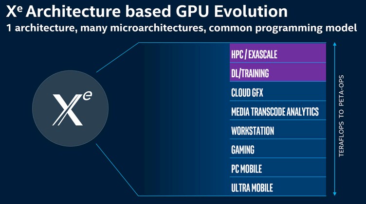
The Xe line of GPUs, which Intel first started to talk about in December 2018, will, we think, borrow ideas both from Knights manycore processors and from the HD, Iris, Iris Pro. Iris Plus and UHD GPUs used in client, workstation, and low-end server devices for the past decade. And, of course, we expect that the Xe GPUs have a slew of new ideas that Raja Koduri, the chief architect of AMD’s GPU processors who joined Intel in November 2017 to do the same job, and his team come up with.
The assumption we made last year was that the Gen11 UHD GPUs used in client chips would be the architectural foundation of the Xe GPUs, but that may not necessarily be the case at all now that we think about it.
The Gen11 GPUs have 72 execution units, which are broken up into three different slices, each with 24 execution units and the slices are broken down further into sub-slices that have eight execution units on them. Because of yield issues, only eight of the cores are presumed to be active, which leaves a total of 64 execution units being balanced out against eight banks of embedded DRAM L3 cache memory that totals up to 3 MB across the whole monolithic chip. These integrated GPUs use a chunk of DRAM main memory in the system as their own memory. To make an Xe discrete GPU, Intel could just break a bunch of Gen12 GPU execution units separate from each other in banks of eight or sixteen, stitch the tiles together using its Embedded Multi-die Interconnect Bridge (EMIB) technology, and stack up some kind of high bandwidth memory next to this processing complex on a substrate package using its Foveros chip stacking packaging techniques, first disclosed last December as well.
But it may not be that simple. Intel could come up with a totally different GPU architecture that mixes different kinds of compute elements on chips, much as Nvidia has 32-bit integer, 32-bit floating point, 64-bit floating point, and Tensor Core matrix math units all on the same device, working side by side with any three out of the five being able to have work dispatched to them at the same time. It’s really like cramming five different accelerators on the same die, when you think about it, with coherent memory and shared interconnect. This is more complex than trying to keep adding functions to the AVX-512 unit, as Intel is doing in the Xeon SP processors to support 16-bit floating point and soon bfloat16 floating point instructions. Our point is, don’t assume that the Xe discrete GPUs will look like the a UHD 630 GPU on a Xeon or Core chip busted up into chiplets with some fast memory attached to it. It could be a very different animal. Or at least a bigger one with different architectural colors painted on it.
Intel is hosting its HPC DevCon in Denver just before the SC19 supercomputing conference kicks off, and in fact, it looks more like the Xe GPUs will be a line of chips that share a common architecture and a common programming model, but with many different microarchitectures – much as the Core and Xeon or Atom and Xeon Phi architectures had a lot of commonality with some pretty big microarchitecture differences (or if comparing Atom to the others) actual macroarchitecture differences. Technically, they are all X86 processors that can run the same compiled X86 code.
In a briefing ahead of SC19, Ari Rauch, general manager of the graphics business and the visual graphics team within the Intel Architecture, Graphics and Software division at the chip maker, talked a bit about Intel’s intent with the Xe GPU line and also divulged a few details about the Xe discrete GPU that is codenamed “Ponte Vecchio,” after the famous covered bridge that crosses the Arno river in Florence, Italy, that will be etched using 7 nanometer technologies and deployed as the dominant compute engine in the exascale-class Aurora A21 system at Argonne in 2021.
“Several years ago at Intel, we saw a need for developing one graphics architecture that will enable us to scale from the traditional workloads that GPUs were used for all the way to the new scale of performance that are manifesting themselves in exascale capabilities in the HPC and AI training markets,” Rauch explained. “It was fundamental to us that it must be one architecture, and we wanted one architecture because we were thinking about the developers.”
The idea expands beyond Intel GPUs, and its oneAPI effort, which will span all of the four different kinds of compute at compute at Intel, is also intended to be offered as an open standard for the rest of the industry to adopt. So in theory, oneAPI can work on Nvidia GPUs or AMD CPUs and GPUs or Xilinx FPGAs, too. (We shall see.)
There is a subtle change in the chart above compared to the one that was presented back in December 2018. Well, two. Take a look at the old chart:
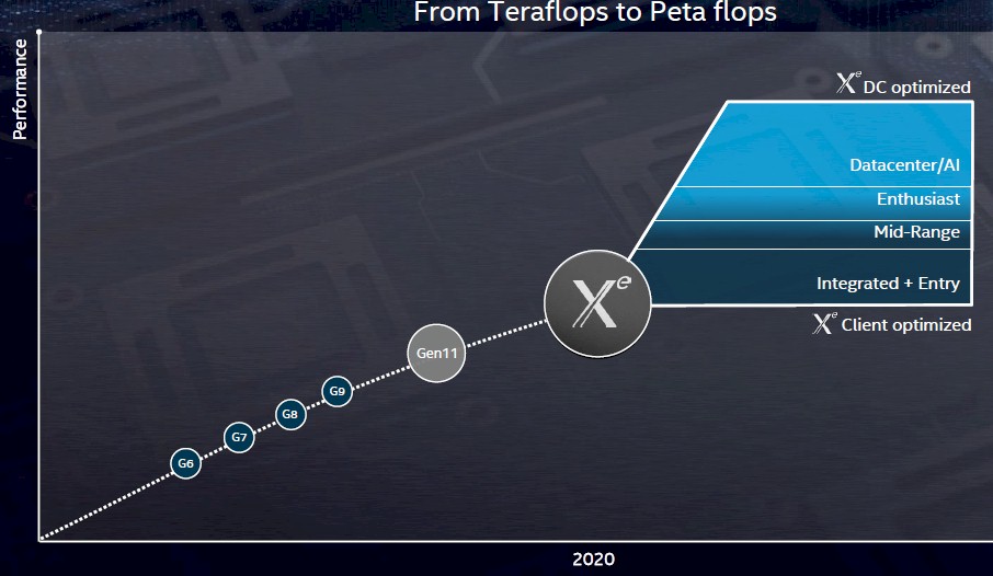
The first subtle change is that there is no prior reference to the Gen6 through Gen11 embedded GPU designs from Intel. That may or may not mean something. The other change is that Intel altered “From Teraflops to Petaflops” on the old chart to now say “Teraflops to Peta-Ops” in the new one. This is a big difference. We did not think that Intel could deliver petaflops of performance, even at single precision, on a single discrete Xe device.
But if Intel has cooked up some sort of analog to the Tensor Core matrix math unit – which it pretty much has to do if it wants to steal business away from Nvidia – the it would be talking about peta-ops at very low integer precision – perhaps INT2 or INT4, for instance. The Nvidia Volta GV100 GPU, for instance, delivers 7.8 teraflops with the FP64 units, 15.7 teraflops with the FP32 units, 31.4 teraflops with FP16 data being double-pumped through the FP32 units, 62.8 teraops (that is ops not flops) through the INT8 units, and 125 teraops through the Tensor Core units, which input data in FP16 format and produce a 4x4x4 matrix math result in FP32 format. If Intel had a Tensor Core analog and put four times as many of them on the die (or made them slightly larger and had fewer of them), it could easily hit 1 petaops of performance. Well, maybe not easily. But at 7 nanometers, maybe Intel can do something like that, particularly with a chiplet approach. The normal SP and DP functions on each chiplet would scale as Intel saw fit depending on application need, the cost of those units on each chiplet, and the price it can reasonably charge for a compute complex with various numbers of chiplets and memory capacity on the GPU package.
Rauch did not discuss the length and breadth of the Xe line, but rather just some of the aspects of the Ponte Vecchio discrete GPU that will be aimed at HPC and AI customers. And it looks a bit like what we are surmising, at least for the HPC and AI variant of the Xe GPU.
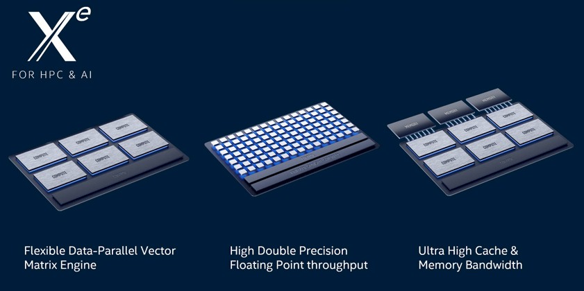
As for what is on those chiplets, the first element is what Intel calls flexible, data parallel, vector matrix engines, and it also includes double precision floating point with a lot of throughput as well as very high cache and DRAM memory bandwidth.
“We built cores that are really flexible in driving data parallel acceleration of work, and this is really adding a lot of capabilities with the high double precision floating point and the throughput,” said Rauch. “We never let go of the need to deliver ultrahigh memory bandwidth for those workloads. This is what is unique about the Xe microarchitecture for HPC and AI.”
It is also what is unique about all GPU accelerators, and even a few CPUs and vector engines now that we think about it, so there is that.
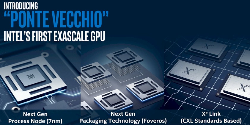
During the briefing, Intel confirmed that the Ponte Vecchio Xe would use the Foveros technology to stack chips on the package and that the compute chiplets on this Xe device would be made using 7 nanometer technologies; the chips will link to processors using a variant of the CXL superset of PCI-Express that Intel has created, and this variant is being called Xe Link. We are not sure what makes it distinct from CXL, which we covered in detail here.
Separately Intel has confirmed to The Next Platform that the Ponte Vecchio discrete GPU will also use EMIB to interlink chiplets inside the Xe package, and also that the device will employ HBM memory like Nvidia and AMD GPUs do as well as Fujitsu’s A64FX Arm processor and NEC’s Aurora vector accelerator. We don’t know if it will be the current HBM2 or impending HBM2E variant; as far as we know, no one has put forth the HBM3 standard as yet.


Keeping Pace In A Fast-Moving AI Space
During the Intel AI Summit earlier this month where the company demonstrated its initial processors for artificial intelligence training and inference workloads, Naveen Rao, corporate vice president and general manager of the Artificial Intelligence Products Group at Intel, spoke about the rapid pace of evolution in the AI space that …
The Irony Of AWS Being Intel’s Latest Savior
Intel needs a whole lot of big wins for both its chip design and selling business and its increasingly arm’s length foundry business if it is going to turn itself around and be competitive with AMD and Nvidia on the left hand and with Taiwan Semiconductor Manufacturing Co on its …
AMD Finally Reaps The Fortunes It Has Sown
Sometimes, competing for business means coming up with better products than your rivals. And other times, competing means just not screwing up while your competitor stumbles. For the heated battle between AMD and its archrival, Intel, when it comes to compute engines in the datacenter, AMD is in the fortunate …
Chiplets in a GPU seems like a good idea, but the memory hierarchy could be challenging for more than a few chiplets per package. This will be Intel’s first dive into this revamped architecture, and they are going up against AMD and Nvidia each putting out refinements to architectures in development for a decade or more. It will be interesting to see how it stacks up when numbers start coming out. I also really want to hear more about the programing model. Cuda isn’t perfect, but Nvidia has had a long time to polish it, and a long time to train users on how to put it to best use. Even if Intel comes up with a good accelerator programming model, it will take a good deal of time and effort to capture mind-share (and market share) from Cuda.
“Technically, they are all X86 processors that can run the same compiled X86 code”
Wouldn’t it be interesting for new processors to run also WASM opcodes?
GPU chiplets are the next logical step, and very much so for Die/Wafer yield issues, as with the actual Monolithic GPUs already being made up of individual independently operating units in the first place. So taking those on monolithic die hosted units and splitting them up across smaller GPU Die/Chiplets is just a matter of reworking the on monolithic die fabric onto some Interposer(Silicon/PCB/Other) substrate and rerouting the traces on the Interposer via bumps to the GPU Die Chiplets hosted above.
Now that’s going to only scale to maybe 8 separate GPU Die/Chiplets before the routing becomes an issue, so for larger numbers of GPU Die Chiplets than 8 that’s going to require a more active interposer and a Network on a Chip/Module solution with more development time required to successfully pull off.
Nvidia has its NVLink and newer Magnmum IO IP to make use of while AMD has its Infinity Fabric IP and Intel its Intel Foveros IP and Compute eXpress Link (CXL) for Intel’s Ponte Vecchio Xe.
AMD has already made use of some of its Infinity Fabric based IP on its Vega 20 Based Radeon Instinct MI50/MI60 SKUs in a similar manner to Nvidia’s NVLink. And AMD, for Apple’s New Mac Pro, has with those semi-custom Radeon Vega II Pro and Radeon Vega II Pro Duo offerings brought that Infinity Fabric IP to use in the Workstation market. For the Radeon Vega II Pro Duo, AMD, for Apple, is already using Infinity Fabric traces to interface 2, Vega 20, DIEs across a single Card’s PCB. And that’s for 2 rather large GPU DIEs with all the Radeon Vega II Pro SKUs also supporting 2 off GPU Card xGMI(Infinity Fabric Links) as well for interfacing multiple Radeon Vega II Pro(Single or Duo) GPU Cards.
So that sort of scaling on currently the Apple Mac Pro 2019 offerings is a start to what will become the interfacing of smaller more modular GPU Die/Chiplet designs from AMD. And Nvidia’s has its own research as well as Intel for GPU Die/Chiplet based designs sometime in the future as the entire market CPUs/GPUs and FPGA/Other products make the transition to full on heterogeneous processor designs.
Processor Die/Chiplets are already proven a success story for AMD in the form of CPUs with Epyc/Naples and even more so for Epyc/Rome with all the advantages of those Epyc/Rome smaller Die/Chiplets and their Die/Wafer yield advantages at 7nm, with the addition to that, Epyc/Rome’s reworked MCM Die topology that moves the memory/IO channels to a 12nm I/O die and reduces the NUMA domain requirements on the Zeb-2 based Rome offerings. And Monolithic GPUs are already too large for optimal Die/Wafer yields what with GPUs being some of the largest monolithic processor tapeouts achieved until very recently.
So the move to GPU chiplets will be accelerated by the economics of the entire processor production process and the need to remain competitive. AMD has already proven that process correct with its Generatons of Zen CPU offerings and the total per socket core counts(64 per socket) with Epyc/Rome and Intel unable to match that with any monolithic design.
Whichever GPU maker that can get to modular scalable GPU designs first will take the high ground for the vary same reasons that AMD did with its Zen based modular CPU Die/Chiplet designs in the x86 CPU market.