
Even before it launched a $1.3 billion acquisition of Cray back in May, Hewlett Packard Enterprise has had exascale aspirations. Its memory-centric concept platform, called The Machine, was a possible contender as starting point for an architecture for an exascale system, and its offshoots based on HPE’s substantial work with the Gen-Z protocol through the US Department of Energy’s PathForward program launched in 2017. The technology is still a little new, and this is perhaps why the three big exascale systems awarded by the DOE have more conventional cluster designs using a mix of CPUs and GPUs and fast system intraconnects and interconnects.
This is also, perhaps, why HPE acquired Cray. Now, HPE has bragging rights for the three big exascale wins in the United States and a customer base into which it can pursue further development of ideas embodied in The Machine, presumably based on the Gen-Z interconnect.
HPE formed the Gen-Z Consortium back in October 2016, just as various kinds of persistent storage with byte-addressable memory capabilities were on the horizon. This is an important distinction. The Machine as well as the more generic Gen-Z protocol uses the load/store semantics of a processor’s main memory, as opposed to the block or file access over the CPU peripheral bus like most storage does inside of a system or across nodes in a cluster.
The idea behind The Machine was to turn the system architecture inside out, to put a giant pool of interconnected memory at the center of the system (really a memory cluster with compute elements hanging off it on the edge), rather than have a core cluster of compute with individual memories hanging off each machine. Gen-Z was supposed to be an open way to bring these ideas to distributed systems, and Dell, Cray, Arm Holdings, Mellanox Technologies, and Xilinx initially all joined up to be among the leadership of the consortium, and so did memory makers Micron Technology, Samsung, Renesas, and SK Hynix. The Gen-Z Consortium has released a total of nine specifications and five draft specifications for all manner of devices in the past three years, and now has 70 members in the hardware and software communities, importantly including Microsoft and Red Hat among operating system suppliers Google and Microsoft among the hyperscalers and cloud builders.
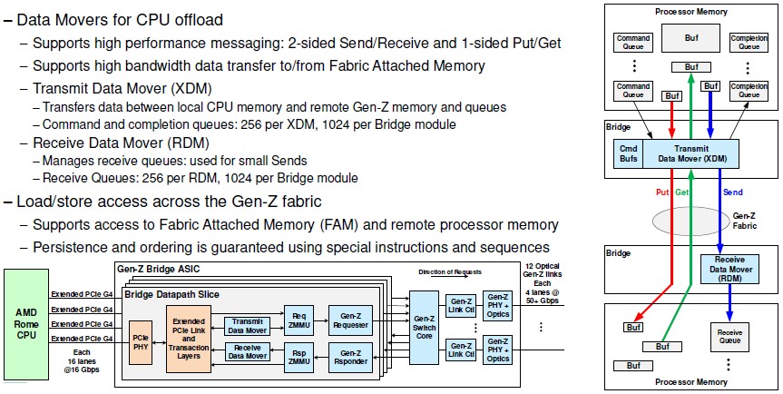
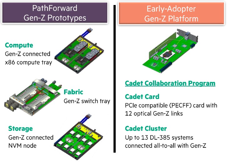
HPE has been talking about its Gen-Z hardware conceptually for years, but having done the work for PathForward as part of the exascale effort, the company actually trotted out the chips used in Gen-Z server bridges and Gen-Z switches, as well as the Hyper-X topology that HPE is recommending for memory-centric clusters. HPE is now putting these devices into a baby cluster, code-named “Cadet” with a mere thirteen nodes based on AMD’s new “Rome” Epyc 7002 processors, to do its initial testing of Gen-Z interconnects and the memory atomics that it allows across compute and storage. Patrick Knebel, an HPE Fellow and vice president in the Silicon Design Lab in the Office of the CTO at the IT supplier, was the one who was tapped from the HPE team to walk through the feeds and speeds. The devices are conceptually very close to the HPC-inspired iterations of The Machine that the company was showing off as a concept back in the summer of 2015 at the International Supercomputing conference in Germany.
“We built this chipset for high performance computing and exascale, but we had to satisfy the needs of our enterprise customers as well,” explained Knebel in a session at the recent Hot Chips conference at Stanford University. “HPE has a very broad portfolio, and this technology has been designed to span the range of that portfolio. Big data analytics, machine learning, simulation and modeling – these just a few of the kinds of applications that our customers are running that are very data intensive workloads. As they adopt more of these workloads, these dataset sizes are providing computational intensity and they’re putting tremendous bandwidth demands on the interconnects for these applications that have lots of node-to-node traffic.”
The upshot is that large enterprises will need some of the same technologies as traditional HPC shops and evolving AI shops, and with the triple whammy of these three areas, a technology that has high performance, reasonable cost, and broad applicability has a better chance to go mainstream – and to make HPE a little money perhaps, too.
Gen-Z can support a lot of different topologies, where they are point to point links between devices or a bunch of devices hanging off of a switched fabric, and the network topology can be a traditional fat tree of a folded Clos, or even the Hyper-X variant of a folded Clos that HPE prefers. The company is testing a cluster with an all-to-all topology (you could think of it as a 1D Hyper-X, we suppose), as shown in the chart below, but expects for an exascale-class system would utilize a 3D Hyper-X topology. The thing about Hyper-X is that it is an all-to-all connection between devices, you can add multiple dimensions to the Hyper-X topology to increase scale and multiple planes to provide cluster resilience and multipathing to deal with traffic congestion on the network.
HPE is all in with optical writing between devices with both The Machine and the Gen-Z prototype, unlike many supercomputing interconnects that use copper cabling in podded up racks and then optical links across pods. Cray’s Dragonfly topology uses such a mix of copper and optical cabling, but it is generally using the MPI protocol to loosely couple cores and their associated DRAM on distinct machines, not trying to do actual memory addressing over the fabric. Electrical interfaces – in this case a pod of four PCI-Express 4.0 ports providing an aggregate of 128 GB/sec of bandwidth – are used to link a server to the Gen-Z bridge chip. The optical interfaces between these bridge chips and the Gen-Z switches implement a proprietary four-lane Gen-Z link that runs at 53 Gb/sec and delivers 318 GB/sec of bandwidth into and out of the switches.
The Gen-Z switch ASIC is implemented in the 16 nanometer processes from Taiwan Semiconductor Manufacturing Corp, using its chip on wafer on substrate 2.5D chip packaging technique (the same one used on graphics cards from Nvidia and AMD), can drive 60 ports with integrated optics, which is a fairly high radix switch considering the bandwidth per port, producing an aggregate of 12.7 Tb/sec of bandwidth. (That’s four lanes operating at 53.1 Gb/sec per port times 60 ports.) That twice the aggregate bandwidth of the most common Ethernet datacenter switches that ship today, which drive 6.4 Tb/sec, and on par with the 12.8 Tb/sec devices that Innovium, Broadcom, Barefoot Networks, and Marvell have announced. (As far as we know, only Innovium is actually shipping a 12.8 Tb/sec ASIC.) The 2D Hyper-X mesh can support up to 3,840 nodes in a 2D mesh with three hops between devices and can stretch to 61,440 devices with four hops and another layer of networking plus a little more latency.
There is a lot of cleverness in the way that HPE has created its Gen-Z chippery, but one of the neat bits is the way it has consolidated the tapeout of the interconnect SERDES for the optical adapters, the bridge core for the server host adapters, and the switch ASIC down to a single area on a wafer. These are cut up and reassembled into packages with eh configurations set as needed. Let’s start with the chip and get into the details:
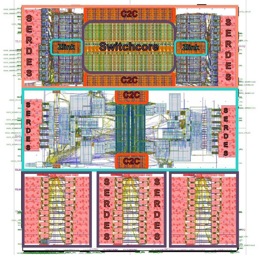
There are five chips sharing this die, and they are sawed free from each other after each etching. The core switch chip is on top, which has communication SERDES and the left and right and chip-to-chip interconnects on the edges top and bottom. (More on these in a second.) The center chip is used in the host bridges, linking four PCI-Express 4.0 x16 lanes – yes, that is a lot, but talking to memory across the fabric, you need it – into the bridge, which hooks into the Gen-Z switch fabric. The bottom three chips are SERDES blocks used for the electrical to optical interconnects that will be used to hook up blocks of DRAM, persistent memory, or flash to the Gen-Z fabric. The Gen-Z bridge chip has electrical SERDES and the Gen-Z switch die has optical SERDES; the electrical to optical dies on the bottom are known as E2O, which is smart enough.
The initial Gen-Z switch chip package has five of the switchcore chips stacked up, linked by their chip-to-chip interconnect edges, like this:
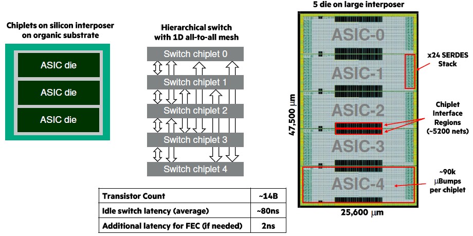
Each chiplet in the five chip stack has around 2.8 billion transistors and implements a dozen Gen-Z ports. It is obviously a lot easier to get good yield on these smaller chips – 25.6 millimeters wide by 9.5 millimeters high – than it would be to create a single monolithic chip with the same functions and about five times the area. (You would be able to lose the chip to chip interconnect, which as you can see adds a little bit of area to the overall design, but you would have to add in a ring interconnect or something else, so it might be a net wash.) The whole complex stacked up has 14 billion transistors, or about 22 percent fewer than Nvidia’s “Volta” GV100 GPU. The five chiplets are linked to each other in a 1D, all-to-all mesh. The idle switch latency in passing through the Gen-Z switch complex is around 80 nanoseconds in a port to port hop, and if you want to add forward error correction (FEC), then add another 2 nanoseconds.
These switch chiplets have fully buffered crossbars, and they implement cross-point buffering to eliminate ingress conflicts and cut back on arbitration complexity. Each chiplet has 16 virtual channels to allow for different classes of traffic, and each virtual channel can be programmed to have multiple primary and secondary routes, depending on the number of planes in each dimension of the Hyper-X topology. Each ingress port has its own routing table, and it includes adaptive routing per packet based on egress congestion and delivers high throughput, according to Knebel, even with small packet sizes.
Here is the schematics for the Gen-Z bridge chip:
And here is how you make the three different potential components in a Gen-Z switched fabric with compute, memory, and other storage:
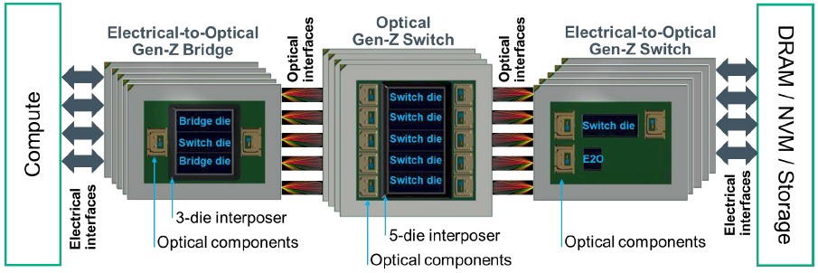
The electrical to optical bridge chip eats those four PCI-Express 4.0 x16 slots coming off the server, aggregating their bandwidth. It has a single switch chiplet, a pair of bridge chiplets, and a pair of the E2O optical connectors on the package, which looks like this:
In the middle of the schematic above, the Gen-Z optical switch has those five switch chiplets stacked up on a package plus ten of the optical SERDES, driving those 60 ports on the switch. Here is what the switch package looks like:
To make an electrical to optical switch, as shown on the right, you have a switch die and one E20 SERDES modules. (We don’t have a sample of this unit.) The E2O Switch Module has a switch die that directly interfaces to the optical components on the module. Thus, HPE does not need an E2O die for fabric-facing functionality, but does need one E2O die on the media-facing side for converting from optical Gen–Z to electrical Gen–Z for connection to those media devices.
Here is the important bit about Gen-Z switching: The optics are integrated with the Gen-Z switching, and the SERDES in the switch package directly drive the optical signals out of and receive the optical signals into the chip complex. Traditional switching using optical links for longer distance or higher bandwidth have to push signals over PCB traces from the switch ASIC to the ports, then they have to jump into high powered transceivers that push the signal over single-mode or multi-mode optical fiber, then catch it with another hot transceiver that receives the signal and converts it back to electrical signals and pushes it over PCB traces back into the other switch ASIC. This costs more money (or will when Gen-Z technologies are mainstream, HPE hopes) and burns more power.
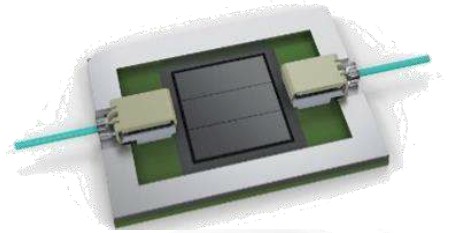
HPE has not put out much detail about its PathFoward exascale project with the DOE, but the prototype that the company no doubt used as part of its bids for exascale deals in the United States had an X86 sled with two single-socket nodes and two Gen-Z bridge chips per tray, plus a Gen-Z switch fabric tray with what looks like two switches:
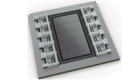
The PathForward work also had a non-volatile storage media tray with eight media drives plus two E2O switches to link that storage into the Gen-Z fabric.
The Cadet early adopter program is simpler, providing a very fat PCI-Express adapter card that implements the Gen-Z bridge to link thirteen of HPE’s two-socket ProLiant DL385 systems using the Rome Epyc processors. The server nodes are linked in an all-to-all 2D Hyper-X topology.
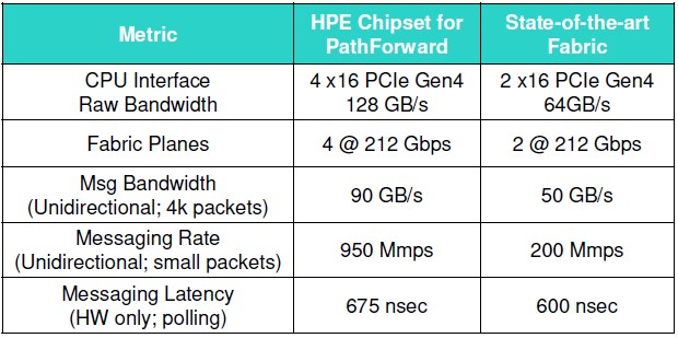
It is not clear which fabric HPE is comparing itself to in the table below, but it looks to be a cherry picking of stats from various interconnects and it clearly shows that the Gen-Z bridge has some advantages over what we presume is an InfiniBand host bus adapter. The key statistic, says Knebel, is that messaging rate.
And to make the point of how this might translate into better application performance, Knebel took out a profile of a genome assembly application from SC15. With this genomics application, data is parsed into genetic sequences of variable length (called k-mers), sorted into contiguous sequences (called contigs), and then aligned, and then scaffolded up into overlapping nucleotides. The three middle steps take up 85 percent of the compute time and are severely limited by communication bottlenecks inside the system and across the interconnect. With that 4.75X higher messaging rate, it is – in theory, based on Amdahl’s Law – possible to speed the overall application up by 3X. HPE has not yet proved this, mind you.
The other thing is that HPE expects for its Gen-Z optical switches and host bridges will be “cost competitive” with high-end HPC fabrics with switches and network interface cards. The Gen-Z devices have twice the bandwidth and almost five times the messaging rates, and it is not clear if HPE plans to price based on units or bandwidth when it says it will be cost competitive.
Looking ahead, HPE is working towards adopting PCI-Express 5.0 ports on its bridge chips and going to 400 Gb/sec signaling on its fabric, and expects to more than double the messaging rate in the next generation of the Gen-Z fabric. Knebel says HPE is looking to shave down the latency on its messaging as well. HPE is also looking at boosting the Cadet cluster with a 4D Hyper-X topology to boost its size to 256 nodes.
It will be interesting to see what HPE does with Gen-Z after it finishes acquiring Cray. It will have cray’s “Slingshot” HPC variant of Ethernet plus this Gen-Z stuff. It is not clear if they can be mixed and matched in some fashion, but Gen-Z could certainly be used to connect nodes to memory and storage pools and Slingshot could be used to link nodes to each other in a distributed system.

HPE Creates Its Own AI Stack For Large Enterprises
While the hyperscalers have been running AI workloads against vast datasets in production for a decade and a half, many large enterprises have lots of data they think is relevant but they are not at all experiences with AI and the system requirements it has. That’s where companies like Hewlett …
Arrow Hits the Mark for Petabyte-Class Analytics Problems
When we first talked to Voltron Data following their launch in early 2022, we had to take care to explain why Apache Arrow was worth paying attention to and why it might warrant the level of enterprise support the startup promised. Even more explanation was needed to justify the $110 …

HPE Further Blurs The Storage Line Between On Premises And The Cloud
The coronavirus pandemic has obviously had an impact on spending trends in the IT market. As businesses temporarily shut their doors and sent most of their employees away to work from home, executives and IT administrators had to almost overnight shift their business model to adapt to a highly distributed …
If Gen-Z is “load/store semantics”, then what is the cache-coherency story? And what is the load/store latency?
Memory coherency does not scale. In S/W it requires virtual memory address sharing, crippled
across processes, impossible across nodes. In H/W for consistency it requires snooping and
invalidation/eviction which cannot cross fault domains without causing halts. Ultimately the
story at scale will be treating shared memory like really fast low-latency I/O, with the
typical base + offset addressing we all use for log records and btree blocks and the like.
Abandon the attachments to virtual memory and coherency. L4TM O/S implemented fabric atomics
(Like CAS and ADD in RDMA), but they will always be flaky. Learn to orchestrate and
choreograph your distributed sorts, etc., with grand layout schemes and Gen-Z memory mail
for cross node in-memory data queuing: like the US patent application 20190095340. Latency
will depend upon near vs. far on the switching fabric (hence the high switch radix,) and
persistence, which for central shared DRAM only requires a battery or UPS, because machine
check or panic forced reboots do not cause central shared memory to be wiped, as is the case
for motherboard attached DRAM.