It has been a long time coming: The day when AMD can put a processor up against any Xeon that Intel can deliver and absolutely compete on technology, price, predictability of availability, and consistency of roadmap looking ahead.
With the second generation “Rome” Epyc chips, AMD is firmly and forcefully back in servers, and it is most definitely going to eat a whole lot more market share than it could with the first generation “Naples” processors that launched almost precisely two years ago. And a trip to the third generation “Milan” Epyc chips is therefore in the cards two years or less from now, even if AMD won’t quite say that publicly yet. The word on the street is that it is coming in the 2020-2021 timeframe, and if we had to guess it will be late 2020 to early 2021 if AMD and its foundry partners can pull it off. The odds are that these future Milan Epyc chips will plug into the same server sockets that Naples and Rome did, extending the lifecycle of the engineering that AMD’s OEM and ODM server partners have done well into the future.
The Long And Winding Road From Naples To Milan
If you take the A1 autostrada from Naples to Rome, it takes about two and a half hours, depending on traffic and the zaniness of Italian drivers. The high speed train link takes a little more than an hour if you are impatient and risk averse. AMD’s trip from Naples to Rome was a bit longer, at two years, and frankly planning for that trip started a long time ago, which Forrest Norrod, senior vice president and general manager of the Datacenter and Embedded Systems Business Group at AMD, recalled in briefings about how AMD got back into the server game.
AMD, Norrod explained, started preparing the field for a return to servers back in 2012 and got to work outlining what went wrong with the prior several generations of core designs – code-named Bulldozer, Piledriver, Steamroller, and Excavator – that opened up a performance gap between its Opteron server chips and the Xeon processors from its archrival, Intel. With the Zen core that is at the heart of its Ryzen PC and Epyc server chips, AMD went back to the drawing board, and in fact, just after Norrod joined the company in 2014, AMD decided to focus solely on X86 processors and dropped its complementary effort to product Arm server chips. The Zen 2 core that is at the heart of the Rome processors, Norrod said, is derivative of the Zen 1 core that is in Naples – much more so than will be the Zen 3 core that will be employed two years from now in the Milan Epyc chips.
“Our heritage was in making high performance X86 processors,” said Norrod. “And we were going to take where we started with Zen and build on it with Zen 2, and Zen 3, and Zen 4, and Zen 5, and we were going to put a roadmap in place the cadence of which I sincerely hope is going to bore you to death. I want to be absolutely predictable about when we bring things to market. When we introduced the first generation Epycs, we said that two years from now we’re going to be launching the second generation, and the third generation is right on track. So it is boring in terms of when we do what. But I hope we can be very exciting in what we are doing.”
It is safe to say that with the Rome Epyc chips, AMD is going to get the attention of the datacenters of the world, and frankly, there has not been as important of an announcement in Server Land since Intel launched its transformational “Nehalem” Xeons – with many architectural ideas inspired by AMD’s Opterons – back in March 2009. It was that Nehalem launch, combined with the Great Recession and a loss of confidence in AMD’s ability to deliver Opterons on time, that compelled AMD to walk away from the server business. That was a painful and difficult decision, and there are many things in life that can be argued in hindsight that are not so obvious at the moment critical decisions are being made.
AMD’s course with its Zen architecture and the chiplet designs with the Epyc processors is a case in point, and Norrod said as much.
“With Zen 2 in Rome, we were going to double down on core,” Norrod explained. “We knew where the efficiencies and the opportunities were. We just had to at some point make a cut with what we could get done in Zen 1 safely. Zen 2 is in some ways more of a derivative core with much higher IPC uplift because we had ideas that we knew we could do in the original Zen 1 design but we didn’t have time. And then we made the decision – and this was a very difficult decision – to double down on chiplets, to move from the four die strategy that we had in Naples, which was very good from the R&D efficiency. We could do one die that we could use not only for the server product, but for the desktop product. We knew that with 7 nanometer that we could not go after the same strategy. We tried to do what we wanted to do in terms of doubling the core counts and sticking with four dies, but we couldn’t do it. The part would not be affordable, yields would not be good, and speed distributions would not be good. We wouldn’t be addressing some of these NUMA effects. But by the same token, moving to a nine die MCM on an organic substrate using a mixed process technology – it seems like it is a simple, brilliant decision. But let me tell you, it was not an easy decision and we had to make it before we brought the first generation of the processor to market. That was a swallow two times hard and once again throw the dice and commit the company. We made a very informed decision and I think it clearly turned out to be the right decision in retrospect. For us, it is incredibly gratifying to see the Zen 2 core come out even better than the commitments that we made. And the market position of the product has greatly exceeded expectations.”
The Feeds And Speeds
As usual, we will begin our coverage on the Rome Epyc 7002 server chip family launch with the feeds and speeds of the processors that AMD is bringing to market. In subsequent stories, we will do a deep dive on the architecture of the Rome chip, and follow that up with competitive analysis with Intel Xeon SP processors, the market positioning of the chips and the initial machines from OEMs and ODMs that use it, Intel’s response to the launch, and some thoughts about what the future of the Epyc family might hold.
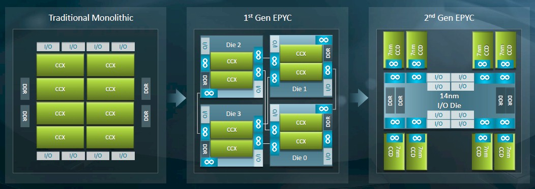
The basic architecture of the Rome multichip module (MCM) was unveiled last November. Rather than having I/O and memory controllers on each chiplet and using PCI-Express ports to create the Infinity Fabric interconnect lashing the dies on the MCM together as was the case with the Naples processor, this time around AMD created a central I/O and memory controller die, etched in the same class of 14 nanometer processes at GlobalFoundries as was the Naples chip, and then hung chiplets containing just core complexes (what AMD calls CCXs). The number of chiplets for these compute cores was not divulged last November, but we now know that each core complex has eight Zen 2 cores and there are eight of them on the Rome package for a total of 64 cores.
Here is what the Naples and Rome packages look like from the outside: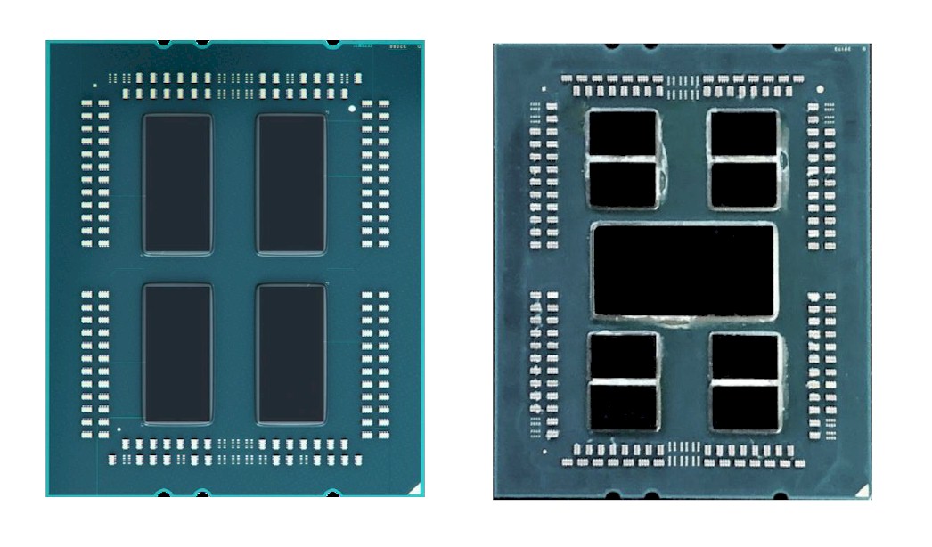 AMD is not providing die shots of either Naples or Rome chiplets or the central hub in the Rome MCM, but we sure wish the company had done so.
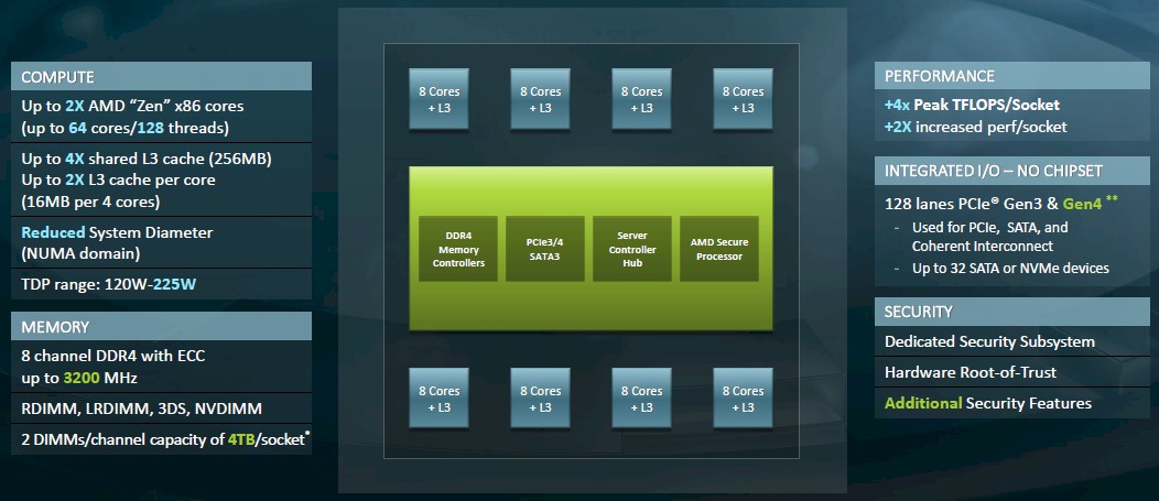
The block diagram further above that shows the complexes seems to imply that there were only four memory controllers on the Naples and Rome chips, but each DDR block is actually a pair of controllers, for a total of eight controllers. The Rome design has 128 lanes of PCI-Express 4.0 I/O that can reach out to peripheral devices and be used as the NUMA interconnect in a two-socket machine; Naples used PCI-Express 3.0 controllers – 128 lanes of them as well – which ran at half the speed and therefore had half the bandwidth. The NUMA coupling with Naples and Rome eats up 64 of the 128 lanes, so a two-socket box with two processors still only has 128 PCI-Express lanes exposed to the outside world. (Technically, there are two extra lanes that are used fort Infinity Fabric control. Count these if you feel like it.) Because all of the chiplets hang off the same I/O and memory hub, which has a fast transport of its own on the die, there is one fewer NUMA hop to get from one chiplet to another, greatly simplifying the NUMA structure of the socket and reducing the overhead of sharing memory across the chiplets in a socket and across sockets. (We will be getting into this separately in our Rome architectural deep dive.)
According to Kevin Lepak, chief architect for the Epyc processor line at AMD, the Rome product line is fleshed out in two ways. Not all of the die sockets on the Rome packages are populated on every SKU, and not every core on each chiplet is fired up based on yields for working cores. The packages can include 2, 4, 6 or 8 chiplets and any number of cores activated to create the Rome product line.
The Rome complex, at a maximum of 64 cores, obviously has twice as many cores as the Naples complex did. The L3 cache on each chiplet has also been boosted in size by 4X to 256 MB, but with twice as many cores on each chip that only works out to 16 MB of L3 cache segmented across four cores, which is still twice as much L3 cache per core as Naples had.
The memory controllers on the I/O hub support two DDR4 DIMMs per channel, up to a maximum speed of 3.2 GHz, and RDIMM, LRDIMM, 3DS, and NVDIMM form factors are supported; obviously, Intel’s Optane 3D XPoint DIMMs are not supported. With two DIMMs per channel and using 256 GB memory sticks, maximum capacity per socket is 4 TB – not that anyone can afford to buy 256 GB memory sticks.
As for raw compute, the top-end Rome chip has 2X the integer performance and 4X the floating point performance as the top-end Naples chip at the same clocks, and SKUs in roughly the same place in the lineup will show similar increases if the cores are doubling up. Mileage will vary by model comparison, of course. And some jumps will hold core counts the same and boost single thread performance. So it is hard to generalize.
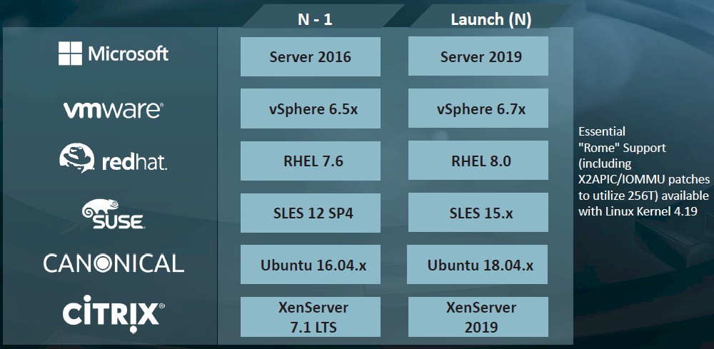
Here is the operating system support for the Rome chips:
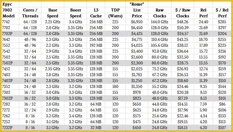
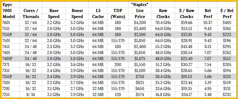
The Rome lineup has fourteen SKUs for two-socket server configurations and another five SKUs that have been designated for single-socket systems and that have had their prices adjusted downwards pretty significantly to allow for AMD to really chase after the belly of the two-socket market with a single socket setup – a strategy that AMD has been espousing since before Naples chips were launched. These single-socket Naples and Rome processors are shown in our tables with gray bars and have a P designation after their name.
So without further ado, here is the Rome Epyc 7002 family of processors from AMD:
And for reference, here are the Naples Epyc 7001 processors:
And for fun, here are the mainstream “Shanghai” Opteron 2300 processors from early 2009 that were launched at about the same time as Intel’s Nehalem Xeon E5500 processors:
Just like we picked the four core, 2.53 GHz Nehalem Xeon E5540 as the touchstone chip against which to measure relative performance across the past eight generations of Xeon processors from Intel, we are picking the Opteron 2387, which also had four cores but running at 2.8 GHz, as the touchstone for all Opteron and Epyc processors. There is not enough time in the day to go all the way back to 2003 for the entire Opteron line, and no point in it anyway. This was the Opteron for two-socket servers that hit the market around the same time as the Nehalem Xeon 5500 series did. We are not saying, by the way, that the Xeon E5540 and the Opteron 2387 have equivalent performance, but we think they are in the same ballpark.
As usual, our rough relative performance metric across these processor lines is cores times clock speed and adjusted by instruction per clock (IPC) increase from generation to generation. We know that IPC increased by 50 percent moving from the last Opteron core (Excavator) to the first Zen 1 core, and that the jump from Zen 1 in Naples to Zen 2 in Rome was another 15 percent on top of that. These are big increases. Historically, Intel gets somewhere between 5 percent and 10 percent more IPC with architectural tweaks between generations; sometimes a little more, and sometimes less. We had to use some pretty rusty benchmarks to estimate the IPC gap between the Shanghai processors and the Naples processors, so take that as you will. We think it is within spitting distance, and certainly enough for the purposes of our discussion.
The Rome lineup spans from the low-end Epyc 7252 and 7232P that have only eight cores fired up, running at 3.1 GHz. And as you can see, these chips have roughly four times the integer performance of that touchstone Shanghai Opteron 2387. There are twice as many cores, and those cores have roughly twice as much IPC, so this stands to reason. The top-end 64-core Epyc 7742 runs at a slower base frequency of 2.3 GHz. But with so many cores it is a throughput dynamo, delivering 24.4X the integer throughput as the Opteron 2387 we set as the baseline. Again, with twice the IPC and 16X the cores, but a much lower clock speed, this stands to reason.
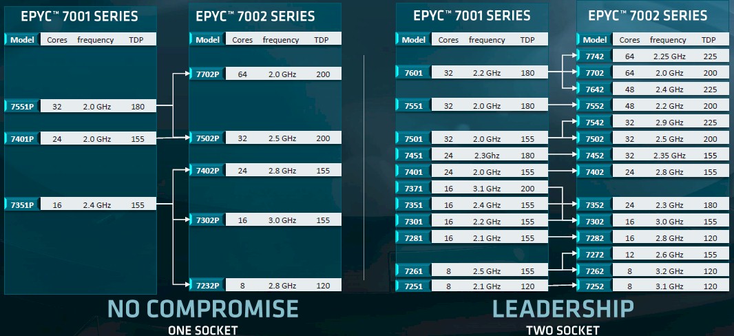
It is very hard to make generalizations across the Naples and Rome lines, but here are a few observations from the SKU stacks for the two lines and the expected upgrade paths, which look like this:
In some cases, the Rome upgrades to a specific Naples chip – and sometimes there are a few – has roughly the same clock speed but more cores and a slightly higher thermal design point. Sometimes the core counts are the same but the clock speeds and wattages go up. Sometimes the clock speeds go up, the core counts are the same, and the wattages also go down thanks to the process shrink on the Rome cores. And sometimes the core counts are the same, the watts are the same, and the clock speeds go way up.
What can be said across the whole Rome line is that it is broader across all of these vectors while still maintaining the simplicity that AMD thinks is vital to customers who are annoyed by paying premiums for successively larger chunks of main memory addressability, support for Optane memory DIMMs, more I/O, or other features. Intel’s Skylake and Cascade Lake Xeon SP processors offer all kinds of choice, but every feature has a price. With AMD Epycs, you get full I/O and memory, all the features, and you are just paying for cores and clocks and watts and sockets. Period. It ain’t complex, and you ain’t getting 5,000 dollared to death on features.
The other thing that is obvious is that AMD is charging more for Rome chips than for Naples chips, but nowhere near the 2X it could charge if price per unit of performance remained essentially flat, Epyc 7001 SKU to closest Epyc 7002 SKU, clock for clock. The market does demand price/performance improvements – when it can get it, of course.
So, for instance, on the top end parts, compare the Rome Epyc 7742 to the Naples Epyc 7601. The Rome chip has twice as many cores (up 100 percent), which run a smidgen 50 MHz faster (2.7 percent), and the IPC on the Rome core yields another 15 percent boost over the Naples core; add that up, and the performance is up by 135 percent, so a little better than 2X you expect based on core counts alone. The watts go up by 25 percent, which is how some of that performance is paid for. But the price only goes up by 65 percent, and that means the price/performance improves by just under 30 percent.
Let’s take a slightly different example, pitting two 32-core Epyc chips with the same 155 watt ratings. That would be the Epyc 7501 running at 2 GHz, which has a relative performance of 9.43 in our rankings of AMD chips, versus the Epyc 7452, which has a relative performance of 12.74. Some of that extra oomph comes from boosting the clock speed to 2.35 GHz – 17.5 percent to be precise – plus there is another 15 percent that comes on top of that thanks to the Zen 2 core IPC improvements. That’s a 32.5 percent increase in performance with the same number of cores and the same 155 watt thermal envelope, and the price rises by 9.5 percent to $2,025. That’s only an 18.9 percent improvement in bang for the buck.
Our point is, there are hundreds of possible combinations across the Rome and Naples Epyc processor lines, and in general, the improvement in bang for the buck ranges from 20 percent to 40 percent, whether the performance jumps are large or small between the Naples and Rome chips compared. Generally speaking, the larger the performance jump, the better the improvement in the value of the upgrade. This is a whole lot better than the reverse situation, where big performance jumps are more costly than little ones.
There is one last thing for now, and that is a shout out to the 16-core Epyc 7282 in the Rome line, which runs at a very respectable 2.8 GHz, costs only $650, and brings the cost per unit of relative performance down to a mere $86. That’s 34.4 percent better bang for the buck than the 16-core Epyc 7182 in the Naples line, which had clocks that only spun at 2.1 GHz and had 34.8 percent less relative performance in our rankings. These two chips are aimed straight into the belly of the Xeon SP Gold processor lineup, and if this specific Naples chip knocked some wind out of Intel, the Rome kicker might bruise a rib or two.
There is lots more analysis to come on AMD’s Rome chip, so stay tuned.




All of AMD’s slides on Milan implies that it is a 2020-product, not a 2021-product as stated in this article.
Yeah it is a slippery thing. The best I can figure, after poking around with some AMD people, is late 2020 to early 2021, but nothing as hard as those images implied.
Supposedly the Zen-# cores for that Frontier Exascale system are not going to be just of the normal Zen-3 variety as that SKU will support CPU to Direct Attached Radeon GPU accelerator interfacing via that AMD xGMI(Infinity Fabric based) IP.
So some custom variant of the Zen-3 design that’s making use of the xGMI(Infinity Fabric) IP that’s been included since Zen-1 but has been only used for Inter-CPU-Die/Inter-Processor-Socket Infinity Fabric communication between CPU sockets on Epyc/Naples and Epyc/Rome(Rome uses IF Version-2 with 2.3 times the per trace bandwidth of IF Version-1).
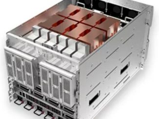
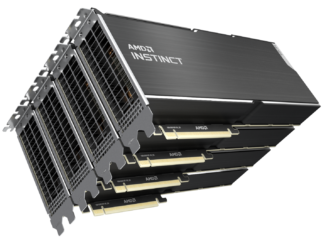
So for the Frontier System there will be One Zen-Custom MCM socket interfaced to 4 Radeon GPUs via an Infinity Fabric protocol based set of xGMI links and one Zen-3/Custom Processor directly interfaced to 4 Radeon GPU compute accelerators via xGMI. And who knows what bandwidth that the Infinity Fabric Version-3 may provide over the IF Version-2 that currently exists for Epyc/Rome.
Maybe by Zen-4 there will be that xGMI(Infinity Fabric) based direct attached GPU accelerator option for all to make use of and some version of the Infinity Fabric that’s much faster than PCIe 5.0 and has a much better set of IF protocol coherency feature sets than PCIe or even CCIX.
There is currently/has been plenty of fast SREDES IP links on AMD’s Zen processor generations and that SERDES is way faster than most external I/O protocols like PCIe/etc. Nvidia/OpenPower has been using that NVLink-2 IP for a while now to interface OpenpPower Power9 CPU sockets to Nvidia’s GPU accelerators and that AMD xGMI/Infinity Fabric IP is AMD’s answer to Nvidia’s NVLink with the only difference being that AMD’s Infinity Fabric was first only used externally to tie Zen/Zen-2 CPU sockets across the Motherboard.
But since AMD’s Vega 20 Generation of 7nm GPUs that xGMI/Infinity Fabric has been enabled for Radeon GPU to Radeon GPU xGMI/IF interfacing on MI50/MI60 SKUs. And since the Vega 10 first generation GPUs all of AMD’s GPU products support the Infinity Fabric IP. So All AMD GPUs going forward from first generation Vega will be Infinity Fabric enabled even if there are no xGMI external links provided on consumer variants currently(Only Radeon Instinct MI50/MI60[Vega 20 based] and Radeon Pro WX[Arcturus/Vega 2 based], and Vega 2 Pro for Apple’s Mac Pro 2019 edition have GPUs with xGMI links provided currently).
Zen-3 is coming in 2020 and competing with Intel’s anticipated 10nm Server offerings and Zen-4 by 2021, which if Intel’s timelines keep slipping for 10nm server SKUs it will be mostly Zen-4 by 2021-2022 anyways. Intel states that they will be on 10nm++ by 2021 but so far only low power mobile 10nm products are announced and shipping to OEMs on that rejiggered 10nm node. Intel had to step back on that 10nm density promise just to get it out the door very late by now what with TSMC and Samsung already getting 5nm ready this year into next.
This is a must watch interview with Lisa Su from The Street Where she states that AMD will be looking to provide the customer options for direct attached GPU accelerator via the Infinity Fabric/xGMI IP at some point in time and not just on that Frontier Exascale custom Zen CPU based platform(1).
So this is definitely going to be competing with Nvidia/OpenPower in the direct attached GPU accelerator market segment. So I’d look into asking AMD about this and directly competing with Nvidia/OpenPower with some Direct Attatched GPU Products/Offerings in a Nvidia/NVLink versus Zen-3/Infiniy-Fabric manner with respect to HPC Pro GPU Compute/AI Accelerator offerings going forward.
I’d really like to read the Next Platform’s take on this as that GPU based AI and compute market along with the usual cloud/server market represents plenty of potential for overall growth and that’s in addition to only taking server CPU market share. And AMD’s already primed with Rome to really take the market share back from Intel on server CPUs but the GPU Accelerator Market and AI/Compute growth and market share is more Nvidia related along with OpenPower as well. That is until Intel gets into the discrete GPU market, Intel already has some FPGA offerings for the AI market as well whereas AMD has no in-house FPGA offerings of its own.
Note: The Cray Question comes at around the 18:53 timestamp in that video and Lisa Su confirms this.
(1)
“AMD CEO Lisa Su Talks New Chips, Confirms She’s Staying: ‘I Have A Lot to Do’
Lisa Su tells TheStreet about AMD’s latest server chips, code-named Rome, and insists ‘we are still in the early innings of the AMD story.’ ”
https://www.thestreet.com/video/amd-ceo-lisa-su-confirms-she-is-staying-15052119
Correction to Edit the 18:53 timestamp to 8:53.
This is a must watch interview with Lisa Su from The Street Where she states that AMD will be looking to provide the customer options for direct attached GPU accelerator via the Infinity Fabric/xGMI IP at some point in time and not just on that Frontier Exascale custom Zen CPU based platform(1).
So this is definitely going to be competing with Nvidia/OpenPower in the direct attached GPU accelerator market segment. So I’d look into asking AMD about this and directly competing with Nvidia/OpenPower with some Direct Attatched GPU Products/Offerings in a Nvidia/NVLink versus Zen-3/Infiniy-Fabric manner with respect to HPC Pro GPU Compute/AI Accelerator offerings going forward.
I’d really like to read the Next Platform’s take on this as that GPU based AI and compute market along with the usual cloud/server market represents plenty of potential for overall growth and that’s in addition to only taking server CPU market share. And AMD’s already primed with Rome to really take the market share back from Intel on server CPUs but the GPU Accelerator Market and AI/Compute growth and market share is more Nvidia related along with OpenPower as well. That is until Intel gets into the discrete GPU market, Intel already has some FPGA offerings for the AI market as well whereas AMD has no in-house FPGA offerings of its own.
Note: The Cray Question comes at around the 8:53 timestamp in that video and Lisa Su confirms this.
(1)
“AMD CEO Lisa Su Talks New Chips, Confirms She’s Staying: ‘I Have A Lot to Do’
Lisa Su tells TheStreet about AMD’s latest server chips, code-named Rome, and insists ‘we are still in the early innings of the AMD story.’ ”
https://www.thestreet.com/video/amd-ceo-lisa-su-confirms-she-is-staying-15052119
OK maybe since Epyc/Naples on through to Epyc/Rome’s release there is now in place that overlapping development cadence to begin a yearly offering of next generation products. So Zen-3’s design has already been frozen and it’s being vetted/certified and can be expected sooner than 2 years.
Since that first Zen-1 Epyc/Naples design was frozen there has been that Zen-2 Epyc/Rome process happening as well in parallel to the Epyc/Naples design/vetting cadence and I’d expect that AMD’s Epyc/Milan will have the same UMA sort of central I/O die topology that Epyc/Rome possesses and the time to market for Epyc/Milan is not going to take as long to be properly vetted/certified and introduced.
So AMD’s server CPU R&D and vetting/certification pipeline is fully saturated with all the various CPU generational processes happening in an overlapping parallel development lockstep cadence for at least 3 generations of products to be concurrently developed and producing a yearly offering of new server products.
Maybe with Zen-3 there can be an even wider order superscalar core and maybe SMT4 and maybe there can be a process node shrink for Epyc/Milan’s I/O die and some large L4 cache to relieve some of that 4 CPU cores to a CCX unit cache size pressure above the CCX Unit’s 16MB allotment. So on Epyc/Rome all traffic must make a hop to the I/O die and any cache needs above 16MB per 4 core CCX Unit begins to incur some latency penalty even if data/code is still in some other CCX unit’s L3 with the larger latency penalty always being DRAM related. So If Epyc/Milan is not going to see any larger per CCX Unit L3 cache size increase then maybe L4 cache can be added to Epyc/Milan’s I/O die with that die on say a 7nm process down from 14nm and plenty of room for more of everything.
I’d even look at maybe some 8 core(CCD) die for Epyc/Milan, or later, where every core on the CCD die shares 32MB of L3 and maybe those 8 cores on a ring bus Infinity Fabric topology and everything between the CCD dies via the I/O die the same as Epyc/Rome. That’s one possible topology that can reduce latency to some degree among 8 cores for Zen-3 and Epyc/Milan, it sure would help for any real time tasks among 8 cores on the same CCD that need a minimal latency(Gaming being one but there are others as well). Maybe that would take until Zen-4 to engineer and vett/cetiify but there is a consumer/gaming market to consider and maybe it’s time for a bifurcation of consumer and server/HPC core designs to some degree from AMD.
L4 cache would be an easy addition that could be added to the I/O die on Epyc/Milan and done so in a transparent fashion to any CCD die designs on Zen-3/later for a great potential latency improvement benefit relative to any DRAM latency costs. Of course increasing the per CCX Unit’s 16MB Cache once again will help there also but that’s going to take more CCD die space to implement relative to some larger L4 cache on the separate I/O die. One of the main benefits for AMD’s CCD/Dual CCX unit die designs is that the CCD die is very small in area and the CCD die/wafer yields are maximized with smaller sizes so maybe the introduction of a large L4 cache on the I/O die is the better option in the longer run and the easiest to implement without to much changes to the overall CCD die’s design. Any large I/O die based L4 Cache would benefit all of Epyc/Milan’s 8 core to 64/larger core offerings as the L4 would be on the I/O die and globally available to any number of CCD’s across any SKU. And the available L3 cache size goes down as the CCD die count is reduced, so a fixed L4 cache on the I/O die could remain constant in size regardless of the CCD die counts across the a range of core count offerings.
With up to 64 cores and 200+ watts per socket, I would expect the ability to run at the turbo clock speed would depend very much on cooling efficiency. That would depend on the air temperature, airflow and heatsink size – which would be challenging in a 1U server.
For any given turbo speed, for heavily multithreaded software sharing memory between the threads, then the bottlenecks will be main memory latency and bandwidth, L3 latency and bandwidth, inter-socket latency and bandwidth and generally the ability of the system to maintain cache coherency.
If the software is not multithreaded, then the data and instructions for each thread are entirely separate. So with 256 threads per dual socket server, cache thrashing and main memory bandwidth and latency would be the primary bottlenecks. Then it would be best to keep each core to a single thread rather than trying to run twice as many threads in the hope that each thread would have better than 50% the throughput.
A lot of these high core count dual socket monster systems are going to be running cloud servers. With competition between the various groups of VMs – each for a different customer – for L3 cache and main memory, I think performance will vary greatly between the ideal circumstance of most other VMs idling and them all trying to run at full capacity.
The days of ever-increasing CPU and memory clock speeds are long gone. The game now is core count, IPC, cache size and memory width, in which these devices excel. However the actual performance is hard to predict since it depends on all the circumstances and the bottlenecks – every one of which the designers surely think about in their sleep:
http://www.firstpr.com.au/misc/Peter-Aschwandens-frontispiece-for-How-to-Keep-Your-Volkswagen-Alive.jpg