
What is the most important factor that will drive the Nvidia datacenter GPU accelerator juggernaut in 2024?
Is it the forthcoming “Blackwell” B100 architecture, which we are certain will offer a leap in performance over the current “Hopper” H100 and its fat memory younger sibling, the H200? No.
Is it the company’s ability to get millions of H100 and B100 GPU chips back from foundry partner Taiwan Semiconductor Manufacturing Co? No it is not.
Is it the Nvidia AI Enterprise software stack with its CUDA programming model and hundreds of libraries and the fact that at least some of this software, if not all, is the de factor standard for AI training and inference. No yet again.
While all of these are certainly massive advantages, and ones that so many competitors have focused their efforts on, the most important factors about Nvidia that will drive its business in 2024 have to do with money. To be specific: Nvidia exited its fiscal 2024 year in January with just a hair under $26 billion in cash and investments in the bank, and if this fiscal year goes as expected, with revenues topping $100 billion and with somewhere north of 50 percent of that showing up as net income, then it will add around $50 billion more to its coffers – even after paying for its taxes and vast research and development operations as well as the normal running of the company.
You can do a whole lot with $75 billion or more, and one of them is not to worry so much about the exorbitant amount of money that will be necessary to buy HBM stacked DRAM memory for datacenter-class GPUs. This memory, which is getting faster, denser (in terms of gigabits per chip), and fatter (in terms of terabytes of bandwidth and gigabytes of capacity) at a pretty good clip, is not improving as fast as AI accelerators need. The supply of HBM, while improving now that Micron Technology has joined SK Hynix and Samsung as suppliers, and the feeds and speeds are improving right alongside of that supply. And we strongly suspect that supply will not meet demand, and pricing on HBM memory will continue to climb right along with the GPU accelerator prices that HBM drives to a certain extent.
AMD, at $5.78 billion in cash and investments, doesn’t have that kind of money laying around, and even though Intel has a little over $25 billion in the bank, it has to build foundries, which are very expensive indeed (on the order of $15 billion to $20 billion a pop these days). So it really can’t afford to splurge on HBM memory, either.
The other factor that plays into the favor of Nvidia’s GPU accelerator business is that at this point in the GenAI boom, customers will pay just about anything for hundreds, thousands, and even tens of thousands of its datacenter GPUs. We think the price of the original “Hopper” H100 GPU announced in March 2022 and specifically in an SXM configuration costs north of $30,000 for a single H100 with 80 GB of HBM3 memory at 3.35 TB/sec, and we do not know what for an H100 with 96 GB of memory at 3.9 TB/sec; we can only speculate what Nvidia could charge for an H200 device with 141 GB of HBM3E memory running at 4.8 TB/sec. By boosting the memory capacity by 76.3 percent and the memory bandwidth by 43.3 percent to make the H200, which is based on the same exact “Hopper” GPU as in the H100s, the performance of the H100 chip rose by between 1.6X and 1.9X. And considering that extra capacity means needing fewer GPUs and burning less juice to training a given model against a static dataset, we think Nvidia could easily charge 1.6X to 1.9X for the H200 compared to the original H100.
The Golden Rule: He Who Has The Gold Makes The Rules
We are not saying that this is what will happen as the H200s start shipping in the second quarter. (We think Nvidia speaks in calendar quarters except for its financials.) We are just saying there is a logic to such a move. A lot depends on what AMD is charging for the “Antares” Instinct MI300X GPU accelerator, which has 192 GB of HBM3 running at 5.2 TB/sec. The MI300X has considerably more raw floating point and integer oomph and a 36.2 percent advantage on HBM capacity over Nvidia’s H200 and a 10.4 percent advantage on bandwidth over the H200.
And you can bet Elon Musk’s last dollar that AMD is in no mood whatsoever to do anything but charge absolutely as much as it can for the MI300X, and there is even a suggestion that the company is working to get an upgrade to fatter and faster HBM3E memory into the field to keep the heat on Nvidia. The MI300 is using HBM3 with eight-high DRAM stacks, and the memory controllers in the MI300 have the signaling and bandwidth capacity to drive twelve-high stacks at a faster HBM3E clock speed. That represents a 50 percent increase in capacity and potentially a 25 percent increase in bandwidth. So that is 288 GB of HBM3E capacity per MI300X and 6.5 TB/sec of bandwidth.
And presumably, such a gussied up MI350X chip, as we might call it, does a proportionately larger amount of actual work against its peak flops – or more, as happened with Nvidia’s jump from the H100 to the H200.
It is against this backdrop that we want to talk about happenings in the HBM space. We will start with SK Hynix, which was showing off an HBM3E stack that was sixteen chips high and delivering 48 GB of capacity and 1.25 TB/sec of bandwidth per stack. With the eight memory controllers as are on the MI300X, that would work out to 384 GB of memory and 9.6 TB/sec of bandwidth. Now we are talking!
With those kinds of numbers, you don’t have to have a CPU as an extended memory controller for a bunch of workloads. . . .
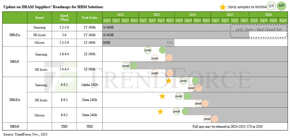
We have not seen the presentation on the SK Hynix sixteen-high HBM3E memory, or have a sense of when it will be available. Last August, SK Hynix was showing off its fifth generation of HBM memory and its first generation of HBM3E memory, which it said delivered 1.15 TB/sec of bandwidth per stack. The expectation, as seen below in the HBM roadmap created by Trendforce, is for this to be available in 24 GB and 36 GB capacities, which implies an eight-high stack and a twelve-high stack.
It was clear last August that Nvidia would be a big customer for these chips, and the word on the street is that this 24 GB HBM3E memory from SK Hynix will be used in the impending “Blackwell” B100 GPU accelerators. If so, that would yield 144 GB across six memory controllers on a Blackwell GPU chiplet, and if the B100 package has two GPU chiplets as expected, that would mean a maximum of 288 GB of capacity with 13.8 TB/sec of bandwidth. It is hard to say how the yield would be, and it is possible that only 5/6ths of this is available. It is also possible – but we hope not – that the B100 does not look like one GPU but two GPUs to system software (just like the two-chiplet AMD “Arcturus” MI250X did and unlike the MI300X does, which has eight smaller GPU chiplets that add up to a lot more oomph and that look like one GPU to system software). We shall see what happens there.
Today, Micron Technology, which is late coming to the HBM game but certainly most welcome on the field given the dearth of supply and the high demand, said today that it was beginning production of its first HBM3E memory, which is an eight-high stack with 24 GB of capacity – and added that the memory is part of the H200 GPU. The Micron variant of HBM3E, which we profiled last July, has pins that run at 9.2 Gb/sec and that deliver 1.2 TB/sec of memory per stack. Micron also claims that its HBM3E memory burns 30 percent less juice than “competitive offerings,” and presumably it is talking about strict HBM3E comparisons there.
![]()
Micron also said that it has begun sampling its twelve-high 36 GB variant of HBM3E, which will run faster than 1.2 TB/sec. How much faster than 1.2 TB/sec, Micron did not say.
Later today, Samsung trotted out its twelve-high stack of HBM3E, also its fifth generation of product and codenamed “Shinebolt” by the company.
Shinebolt replaces the “Icebolt” HBM3 memory launched last year. The Icebolt stacked DRAM memory delivered 819 GB/sec of bandwidth for a twelve-high stack with 24 GB of capacity. The Shinebolt HBM3E delivers 1.25 TB/sec of bandwidth in a 36 GB stack, just like the SK Hynix HBM3E twelve-high stacks do.
Samsung added this interesting tidbit in its announcement: “When used in AI applications, it is estimated that, in comparison to adopting HBM3 8H, the average speed for AI training can be increased by 34 percent while the number of simultaneous users of inference services can be expanded more than 11.5 times.” This is based on internal simulations, not actual AI benchmarks, Samsung noted.
Samsung’s Shinebolt HBM3E 12H is sampling now and full production is expected sometime before the end of June.
These twelve-high and sixteen-high HBM3E stacks are pretty much what we have in store until HBM4 comes out some time in 2026. One could hope HBM4 would happen in 2025, and there is no question there is pressure to move up the roadmap, but this seems unlikely. The speculation is that with HBM4, the memory interface will be doubled up to 2,048 bits. HBM1 through HBM3E have used a 1,024-bit memory interface, the signaling has increased from 1 Gb/sec to 9.2 Gb/sec from the initial HBM memory that AMD designed with SK Hynix and delivered back in 2013. Doubling the interface will allow twice as much memory to hang off the interface and for a given amount of bandwidth to be delivered at half the clock speed and the bandwidth to gradually be raised as clock speeds ascend again. Or. They will just come out at 9.2 Gb/sec per pin from the get-go and we will just pay the price in watts.
The Micron roadmap says that HBM4 will offer capacities of 36 GB and 64 GB and drive 1.5 TB/sec to 2 TB/sec, so it looks like there will be a mix of wide and slow and wide and faster but not full out when it comes to bandwidth. Double the width is how you are nearly doubling up the capacity as well as the bandwidth, it seems. The expectation is that HBM4 will have sixteen-high DRAM stacking and no more.
In a dream world in an alternate universe in 2026, HBM4 would have a 2,048-bit interface, something like 11.6 Gb/sec signaling on the pins with 24 high DRAM stacking with 33.3 percent denser DRAM memory (4 GB instead of 3 GB) and could therefore have something on the order of 3.15 TB/sec per stack and 96 GB per stack. Oh, let’s go crazy then. Let’s say that a GPU complex will have a dozen chiplets, each with their own HBM4 memory controller. That would deliver 37.8 TB/sec of aggregate memory bandwidth per GPU device and 1,152 GB of capacity per device.
To put that into perspective, a 175 billion parameter GPT-3 model, according to Nvidia, needs 175 GB of capacity to do inference, so this memory size on a theoretical GPU we are talking about would presumably be able to handle 1.15 trillion parameters for inference. For training on GPT-3, it took 2.5 TB of memory to load the corpus of data. If you had Hoppers with 80 GB HBM3 memory, you would need 32 of them to do the job. But 32 of our devices would have 14.4X more capacity, and therefore would be able to load a proportionately larger amount of data. The bandwidth on our hypothetical device is 11.3X higher as well.
Notice how we didn’t say anything about flops across those dozen GPU chiplets? Running anything at more than 80 percent utilization is very tricky in most instances, particularly when it might be doing different things at different precisions. What we want is to get the flops to bits/sec ratio back into whack. We want to build a 12 cylinder engine that has enough fuel injectors to actually feed The Beast.
Our guess is that an H100 with 80 GB had about as third as much HBM3 memory as was ideal and about a third the bandwidth, too. This is a way to maximize GPU chip sales and revenue, as Nvidia has clearly demonstrated, but this is not the way to build a balanced compute engine — any more than Intel putting half as many DRAM memory controllers on its X86 chips and selling us all two sockets with middle bin parts was ever the right answer for general purpose computing in the datacenter. We needed more memory capacity and bandwidth there, too.
So if the bandwidth is increasing by 11.3X with this conceptual Beast GPU accelerator, maybe the compute compared to the original H100 only increases by a factor of 4X. An H100 is rated at 67 teraflops at FP64 precision and 1.98 petaflops at FP8 precision (no sparsity used) on the tensor cores. So this TP100 GPU complex would be rated at 268 teraflops at FP64 and 7.92 petaflops at FP8, and each GPU chiplet would be a third of the performance of an H100 chip and would be probably be a quarter to a fifth of the size depending on the process technology used. Let’s say it is TSMC 2N or Intel 14A versus the TSMC 4N used on the real H100. This is 2026 we are talking about, after all.
This is the kind of Beast we want to write about, and if we had $26 billion in the bank and the prospects of another $50 billion plus coming, this is what we would do. But lots of HBM memory and cram the compute engines full of it.
It is hard to say what this would cost. It’s not like you can call up Fry’s Electronics and ask what the street price on HBM4 memory is going to be in 2026. For one thing, Fry’s is dead. And for another, we can’t even get a good sense of what the GPU and other matrix engine makers are paying to HBM2e, HBM3, and HBM3e memory now. Everyone knows – or thinks they know – that the HBM memory and whatever interposer is used to link memory to the device are the two main costs in a modern AI training and inference engine. (This who use a mix of on-chip SRAM and normal DRAM excepted, of course.)
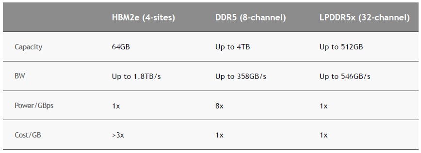
On the street, the biggest, fattest, fastest 256 GB DDR5 memory modules for servers cost around $18,000 running at 4.8 GHz, which works out to around $70 per GB. But skinnier modules that only scale to 32 GB cost only $35 per GB. So that puts HBM2e at around $110 per GB at a “greater than 3X” as the Nvidia chart above shows. That works out to around $10,600 for 96 GB. It is hard to say what the uplift to HBM3 and HBM3E might be worth at the “street price” for the device, but if it is a mere 25 percent uplift to get to HBM3, then of the approximate $30,000 street price of an H100 with 80 GB of capacity, the HBM3 represents $8,800 of that. Moving to 96 GB of HBM3E might raise the memory cost at “street price” to $16,500 because of another 25 percent technology cost uplift and that additional 16 GB of memory and the street price of the H100 96 GB should be around $37,700.
It will be interesting to hear the rumors about what the H200, with 141 GB of capacity (not 144 GB for some reason), might cost. But if this kind of memory price stratification holds – and we realize these are wild estimates – then that 141 GB of HBM3E is worth around $25,000 all by itself. But at such prices, an H200 “street price” would be somewhere around $41,000.
Note: This is not what we think Nvidia is paying for the HBM3 and HBM3E memory – this is not a cost for bill of materials – but an allocation of price to the end user.
We don’t think the uplift can be much more than around 25 percent because the memory upgrade to HBM3 and then HBM3E would push the memory price to be larger than the rumored prices of Nvidia GPUs on the street.
Remember that this is just a thought experiment to show how HBM memory pricing is controlling the number of GPUs that Nvidia and AMD can put into the field, and not the other way around. The memory tail is wagging the GPU dog. The memory capacity and bandwidth are getting more in whack with the H200, and if Nvidia only charges a nominal charge for that extra memory and its extra speed, then not only will the real efficiency of the devices improve, but the price/performance will be significantly improved. But if Nvidia just prices these beefier H100s and H200s so the performance gain and the memory gains balance, there will be much less bang for the buck and much more bucks to be spent.
We honestly do not know what Nvidia will do, or what AMD will do when it gets an HBM3E upgrade for the MI300. With 50 percent more HBM vendors now that Micron is in the field and with SK Hynix and Samsung boosting their output by, say, 2X, which is a lot, that is still only 3X more HBM memory in the market against a demand for GPUs and fatter memory for them that is arguably larger than 3X. This is not an environment where one cuts price. This is an environment where one raises prices on more advanced compute engines and their memories and continues to spread the HBM memory as thinly as one can get away with.
Which is why he who can pay top dollar for HBM memory – that would be Jensen Huang, co-founder and chief executive officer of Nvidia – can set the pace and the price in AI training so long as the Nvidia platform continues to be the preferred one.

H100 GPU Instance Pricing On AWS: Grin And Bear It
UPDATED: It is funny what courses were the most fun and most useful when we look back at college. Both microeconomics and macroeconomics stand out, as does poetry writing, philosophy, and religious studies despite the focus on engineering and American literature. The laws of supply and demand rule our lives …
Datacenter Will Be AMD’s Largest – And Most Profitable – Business
Two and a half years into the global coronavirus pandemic we all have upgraded our home IT infrastructure. And after several fibrillatory interest rate shocks by the major governments to try to curb inflation in the world economy, spending on PCs has consequently taken a nose dive. And a glut …
Nvidia Previews Ampere Kicker To Turing GPU Accelerator
We are still digging through the content coming out of the GTC 2020 fall conference and would be remiss if we didn’t talk a bit about the “Ampere” A40 and A6000 GPU accelerators that Nvidia is previewing. Nvidia has always designed distinct GPUs for different workloads, and some of them …
Outstanding piece (very nuanced)! One thing I’ve been wondering about recently, is whether Intel’s transparent glass substrate (for chips) could be used to ease chip-stacking and interposer (eg. CoWoS) challenges by making it possible to transmit signals optically through it (rather than with copper vias). I can’t remember reading anything on that possibility (maybe far-fetched?), as the tech was pitched at thermal stability I think, but if it also allows for light-signalling, it may help with having to route 2,048 wires from each HBM stack to all nearby CPUs …