

We are still digging through the content coming out of the GTC 2020 fall conference and would be remiss if we didn’t talk a bit about the “Ampere” A40 and A6000 GPU accelerators that Nvidia is previewing.
Nvidia has always designed distinct GPUs for different workloads, and some of them are in the datacenter proper and others end up on the corporate desktop or in a sidecar as what are called “professional graphics.” But increasingly the GPU accelerator is more of a general purpose device and thus the walls are breaking down between graphics, visualization, and rendering with ray tracing acceleration and raw compute as used by AI and HPC workloads. What is consistent, however, is that Nvidia is still creating two distinct families of devices that tune up different aspects of the architecture. In recent years, the lower end GPU had modest 64-bit floating point capability but special cores for doing real time ray tracing, while the higher end GPU had lots of 64-bit oomph and did not include the ray trading cores. In the prior generation, we knew these as two architectures – “Turing” and “Volta” – and really, given this, there are two Ampere implementations of a broader architecture.
A lot of the feeds and speeds of the lower-end Ampere chip are not available, but we will tell you what we know and infer the rest where we can. We can start with the Ampere GA102 and GA104 architectural whitepaper, which Nvidia released concurrent with the GeForce RTX 3080 and 3090 GPU cards, and for you geezers in the crowd, you know why those model numbers are funny. (For those of you who still have your youthful glow, those are the IBM mainframe families from the 1980s and the 1990s, and there is no way that is accidental.) To spread out its risk a bit on the foundry front, Nvidia went with Samsung as its foundry with the Ampere GA102 and GA104 chips, and as far as we know, only the GA102 chip is available at the moment. These chips are etched using 8 nanometer processes, down from the 12 nanometer processes from foundry partner Taiwan Semiconductor Manufacturing Corp that were used to make the prior generation Turing TU102 and TU104 chips for graphics cards and compute accelerators. This 8N process from Samsung is custom to Nvidia, and the two companies are working together to help Samsung learn how to make bigger chips. (IBM is doing the same with the 7 nanometer processes from Samsung with its Power10 chips.)
We only know about the Ampere GA102 chip at this point, and it has 28.3 billion transistors, 52.2 percent more transistors than the Turing TU102 chip it replaces. Given the process shrink, you would expect for there to be around 50 percent more transistors in the same area, but the Samsung process has the added benefit of shrinking the die size by 16.7 percent to 628.4 square millimeters. In general, smaller chips tend to yield better, as do more mature processes.
This is a hedge of sorts, and while we have heard that the limited supplies of the GeForce RTX 3080 and 3090 cards is a demand-exceeding-supply issue, we suspect that the supply was itself a bit curtailed given the foundry shift and the custom 8N process. It’s hard to say for sure. What is clear is that gamers want these Ampere GA102 devices, and we think datacenters will for certain workloads as well – provided the bang for the buck beats the full-on Ampere GA100 devices launched in the A100 accelerators earlier this year. As we pointed out in June with our price/performance analysis, that will be a tall order considering how much work the GA100 GPU can do. It will come down to the price of the A40 and A6000 units and what workload customers are aiming at – and which ones they might be afraid they have to support in the future.
The Ampere GA102 GPU has 84 full streaming multiprocessors, or SMs, which each have 128 FP32 CUDA cores, four of the third-generation Tensor Cores that are in the GA100 GPU as well, one second-generation Ray Tracing (RT) core, and 128 KB of L1 cache memory shared by all of these devices in the SM. A pair of SMs comprises a Texture Processing Cluster, six of these comprise a Graphics Processing Cluster, of which there are seven on the GA102 die, as shown in this block diagram:
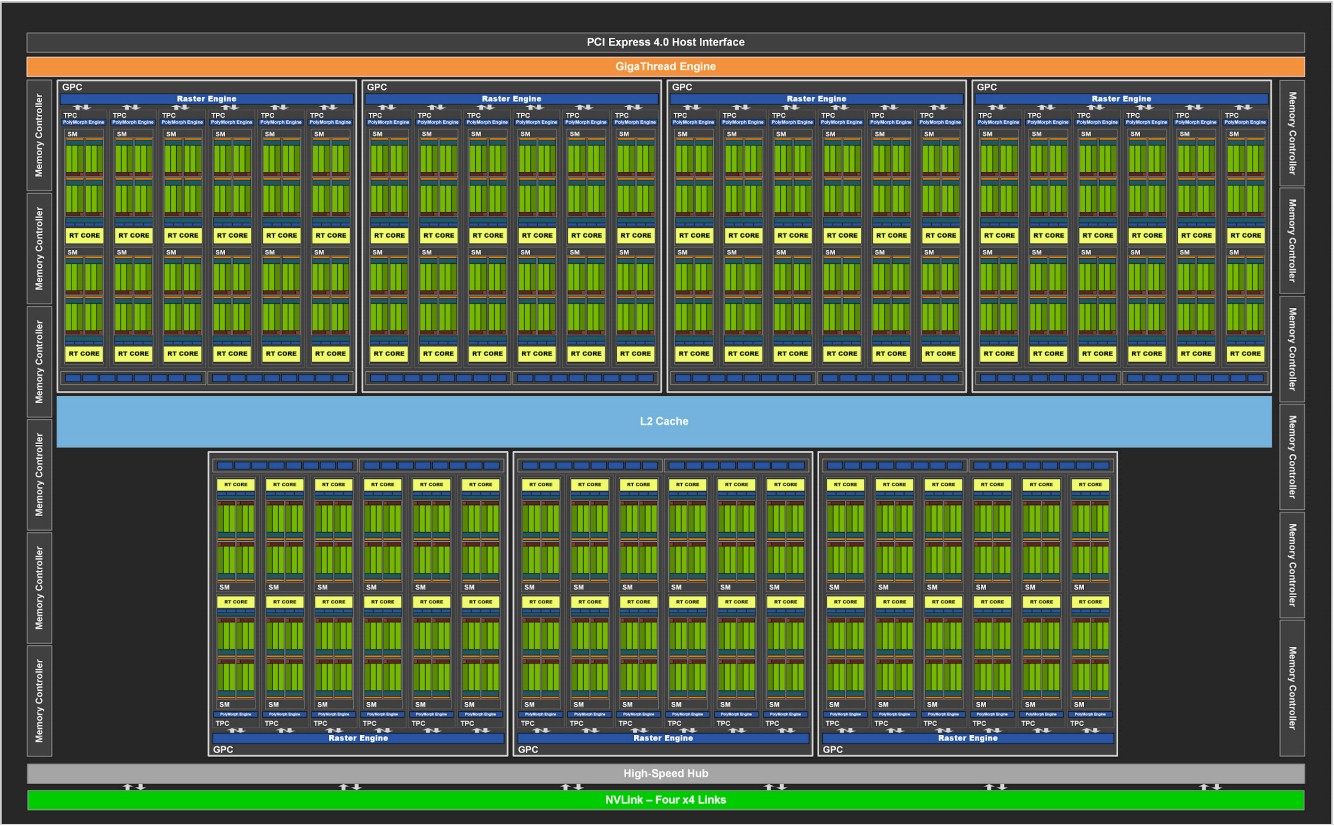
Each SM also has a pair of 64-bit floating point cores, for a total of 168 cores on the GA102 and GA104 dies, and that means the FP64 teraflops rate is 1/64th that of the FP32 CUDA cores, of which there are 10,752 across the entire die. In the case of the A40 and A6000 GPUs, the full complement of SMs and resulting cores are all present and working, although we do not know the clock speed at which they are running and therefore we don’t know the performance, either, except some of the generalities Nvidia has made.
The GA102 GPU has a dozen 32-bit DRAM memory controllers (for a total of 384 bits of width) that have a block of 512 KB of L2 cache associated with each controller, for a total of 6 MB of memory; on the other side of the controllers is 48 GB of GDDR6 memory. On the A60, this GDDR6 memory runs a bit slower and yields 696 GB/sec of bandwidth and on the A6000 card it runs faster and yields 768 GB/sec. On the top end GeForce RTX 3090 graphics card, it runs even faster and delivers 936 GB/sec. The A100 card, with HBM2 stacked memory, is only yielding 1,555 GB/sec by comparison. That extra memory performance of HBM2 versus GDDR6 comes at an engineering and manufacturing cost, for sure. But it is the only way to get that extra 66 percent of memory bandwidth.
The actual layout on the GA102 chip is quite a bit different from the block diagram, as you can see. With the Turing TU102 chip, the SMs were split into two banks, with two NVLink 2.0 ports located in the center of the die. With the Ampere GA102, the NVLink 3.0 ports are down at the bottom of the chip and all of the SMs are stacked on top. The dozen memory controllers wrap around the left, top, and right edges. The NVLink ports are used to lash the memories and therefore the compute of two GPUs together to make a giant, SMP-like virtual graphics card. There is no reason why these NVLink ports could not be used to hang a bunch of A40s or A6000s onto a giant NVSwitch to make a very big and presumably cheap GPU computing complex.
These are pretty hefty devices, at least compared to other GPU accelerators that Nvidia has put into the field. Both the A40, which is conceptually like a beefed up Turing T4 or a radically embiggened “Pascal” P40, and the A6000, which would have been an Ampere-based Quadro professional graphics card for technical and artistic workstations if Nvidia had not done away with the Tesla and Quadro brands recently, both weigh in at 300 watts. That’s a lot given that the “Volta” V100 accelerator from three years ago weighed in at 300 watts and the Ampere A100 comes in at 400 watts, while the T4 comes in at 70 watts.
The RTX 3090 Founders Edition, which has 82 of the 84 SMs on the GA102 graphics engine fired up, runs at a base clock speed of 1,395 MHz and has a GPU Boost overclocking speed of 1,695 MHz; the memory is running at 1,219 MHz. On this chip, the peak FP32 performance is 35.6 teraflops and the peak INT32 performance is 17.8 teraops – neither using Tensor Cores. On the Tensor Cores with FP16 multiplication and FP16 accumulate, the GA102 has 142 teraops and hits 282 teraops when sparse matrix support is turned on and appropriate. For inference, running at INT8 on the Tensor Cores with sparsity support active pushes it up to 568 teraops and at INT4, which is good enough for some machine learning frameworks and which is 4.3X more than the Turing T4’s TU104 INT8; the throughput doubles up again on the Tensor Cores to 1.136 teraops, opening the gap even further.
So with all 84 of the SMs fired up on the GA102, as is the case with the A40 and A6000, then running at the same 1.7 GHz (rounding up) clock speed would mean the GA102 would have 2.4 percent more oomph. But we don’t know what the clock speeds are going to be for either the A40 or the A6000. And based on the thermals, which are 50 watts lower than the 350 watts of the RTX 3090 Founders Edition graphics cards, we think there could be around a 10 percent clock speed shrink to go with that 14 percent wattage decrease. Call it somewhere around an 8 percent less throughout because there are two more SMs in the A40 and A6000 than in the GeForce RTX 3090. Not that you can get either the RTX 3080 or the RTX 3090 right now, but at suggested prices of $699 and $1,499, the A40 and A6000 are going to have to offer some compelling advantages if they are considerably more expensive.
The big difference between the A40 and the A6000 as well as the RTX 3080 and the RTX 3090 is that the former has passive cooling, as shown in the feature image at the top of this story, while the latter three devices have active cooling – meaning they have fans on them. We think it is a geared down A40 that is being embedded on Nvidia’s future BlueField-2X DPU, which we discussed earlier this month. This particular implementation of the GA102 chip would have a whole bunch of its SMs deactivated to only hit 60 teraops – the number depending on the clock speed, the data format, and whether or not sparsity support is taken into account. It could be a lot or a few of the SMs, all depending, and we will try to get it sorted as soon as the information is available.
The RTX A6000 will be available in December through Nvidia’s channel partners, and the A40 is expected to roll out in Q1 2021.


” On the Tensor Cores with FP16 multiplication and FP16 accumulate, the GA102 has 142 teraops and hits 282 teraops when sparse matrix support is turned on and appropriate. ”
Isn’it “On the Tensor Cores with FP32 multiplication and FP16 accumulate …” ?
” On the Tensor Cores with FP16 multiplication and FP16 accumulate, the GA102 has 142 teraops and hits 282 teraops when sparse matrix support is turned on and appropriate. ” Isn’it “On the Tensor Cores with FP16 multiplication and FP32 accumulate …” ?
The architecture whitepaper says it can do both: See Page 38 of this:
https://www.nvidia.com/content/dam/en-zz/Solutions/geforce/ampere/pdf/NVIDIA-ampere-GA102-GPU-Architecture-Whitepaper-V1.pdf
Ah yes !
One advantage of the A6000 over the 3090 would be that you can stack four of them together on one XL-ATX motherboard, regardless of their clock speeds and prices. However, I’m just going to stick with two 3090s until the A6000 is revamped next year with GDDR6X memory and what not.