

With each passing generation of GPU accelerator engines from Nvidia, machine learning drives more and more of the architectural choices and changes and traditional HPC simulation and modeling drives less and less. At least directly. But indirectly, as HPC is increasingly adopting AI techniques, having neural networks learn from real-world or simulated data rather than run a massive calculation predicting the behavior of something, the difference between HPC and AI may be moot in the next decade or so.
This is, in a nutshell, the bet that Nvidia is making as it focuses its GPU compute engines on neural network transformer models and expands its DGX systems to being able to support trillions of parameters in a machine learning training run.
And this bet, we think, is a good thing, since in the long run, if Nvidia is right, more parts of the simulations performed in the HPC centers of the world will be inferred rather than numerically calculated. While dense linear algebra calculations will still be important – notably with simulations providing datasets for physical phenomena that cannot be directly viewed and therefore have no real-world data – the inside of a star or the inside of an internal combustion engine are two good examples – the ratio between single-precision FP32 and double-precision FP64 math and other kinds of math on the GPU is going to continue to shift down to lower precisions.
This has certainly happened with the new 8-bit FP8 floating point format in the new fourth generation Tensor Core that is at the heart of the new “Hopper” GH100 GPU chip from Nvidia. The lower precision data formats in the vector and matrix math units in CPUs and GPUs, including 4-bit and 8-bit integer formats (INT4 and INT8 in the lingo), have not been useful for AI training, but only for AI inference. But with the FP8 format, for many models, a mix of a lot of FP8 and some FP16 with a smattering of FP32 and a taste of FP64 is now sufficient to do training, and FP8 can be used for inference as well without having to do the tedious data conversion to INT4 or INT8 formats for new data to be run against the neural network so it could be identified by the model or converted to another type of data – speech to text, text to speech, video to speech, or speech to video, for example.
It is not hard to imagine a day when Nvidia might be able to create a GPU compute engine that only has floating point matrix math and supports all levels of mixed precision, perhaps all the way down to FP4 and of course all the way up to FP64. But like other compute engine makers, Nvidia has to keep backwards compatibility for software written for its older devices, and that is why we see a mix of 32-bit and 64-bit vector engines (which have the integer support as well as floating point support) and the Tensor Core matrix math engines. We have been cautioned before that there are plenty of calculations that cannot be done efficiently in a matrix unit and vectors will still be necessary. (You will have to pardon our enthusiasm for wanting someone to create the most efficient math engine with no dark silicon.)
The good news is that the streaming multiprocessors, or SMs, in the new “Hopper” GPU have the ability to do math on lots of both vector and matrix data.
SMs are roughly analogous to the cores in a CPU, and in fact, when you look at the core count on a hybrid supercomputer on the Top500 list, that core count is the combination of the number of cores on the CPUs and SMs on the GPUs in that system. SMs have a lot more arithmetic units than CPUs and have schedulers that are explicitly designed to hide latencies across tens of thousands of threads that are comprised of the fairly modest cores that, collectively, provide an order of magnitude or more of performance than CPUs that run at roughly twice the speed. Slower and wider is better for certain kinds of calculations than fast and skinny – at least when you are constrained by chip size, electricity consumption, and heat dissipation and you need to scale up to petascale and now exascale processing.
Here is what the new Hopper SM looks like:

The SM is organized into quadrants, each of which has 16 INT32 units, which deliver mixed precision INT32 and INT8 processing; 32 FP32 units (we do wish Nvidia didn’t call them CUDA cores but CUDA units); and 16 FP64 units. There is a new Tensor Core design, and Nvidia is intentionally obfuscating about the architectural details of this core. Each quadrant has its own scheduler and dispatch unit, which can do 32 threads per clock, and while that scheduler can juggle multiple unit types at the same time, it cannot dispatch to all of them simultaneously. (The ratio with the “Ampere” GA100 GPU was the scheduler could ship work to three out of the five unit types at the same time. We don’t know what it is for the GH100 GPU.) Each Hopper SM quadrant has 16,384 32-bit registers to maintain state of the threads that are being pushed through the quadrant, and eight load/store units and four special function units. Each quadrant has an L0 cache (which sounds like it should be empty, and while it isn’t empty, we don’t know the capacity). The SM is wrapped by a Tensor Memory Accelerator (more on that in a moment), 256 KB of L1 data cache, and an unknown amount of L1 instruction cache. (Why not just tell us?)
It is hard to get the brain wrapped around what a Tensor Core is, but we think of it as a hard-coded matrix math engine where all of the inputs in the matrix go from registers, pour through the unit, and it does all of the multiplication across the matrix elements at the same time and accumulates it in one fell swoop. This is in contrast to lining up some of the vectors individually in the vector units, multiplying them out, stashing the results in the registers, grabbing some more vectors, doing the multiply, and finishing up by accumulating the whole shebang.
Here is how Nvidia illustrated the Pascal matrix math using FP32 units on a 4×4 matrix compared to the Volta Tensor Core units and to the Ampere Tensor Core units, both of which hard-coded the 4×4 matrix math and the latter of which had a sparsity data compression trick that doubled the throughput without sacrificing AI accuracy noticeably:
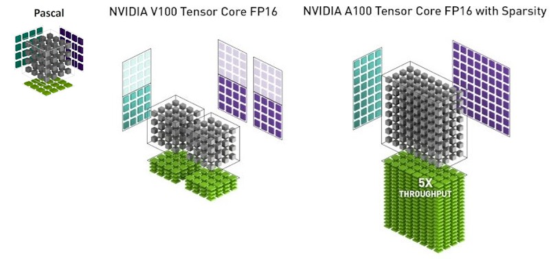
As you can see, the Volta Tensor Core implemented a pair of hard-coded 4×4 matrix by 4×4 matrix multiplies in FP16 mode, with FP32 accumulate. With sparsity on, the A100 Tensor Core effectively became a math unit that was equivalent to doing calculations on a 4×8 matrix multiplied by an 8×8 matrix, yielding a 5X improvement over the V100 Tensor Core.
In the comparison below, Nvidia appears to be showing the Tensor Cores at the SM level for the GA100 and GH100 GPUs, with four Tensor Cores each:
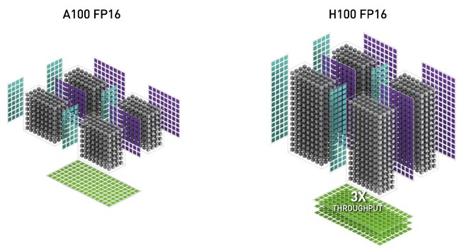
So we know that the GA100 had four Tensor Cores per SM (which Nvidia revealed in its GA100 architecture paper) and we infer from this diagram that the GH100 also has four Tensor Cores per SM (which Nvidia did not disclose in its GH100 architecture paper). And we can also see that in FP16 mode with sparsity on, the Hopper GPU Tensor Core is effectively doing a multiplication of a 4×16 matrix by an 8×16 matrix, which is three times the throughput of the Ampere Tensor Core with sparsity support on.
If you do the math on all of this, and assign the P100 FP64 vector engines a value of 1 multiplying a 4×4 matrix by another 4×4 matrix, then the V100 Tensor Core was 8X more powerful, the A100 Tensor Core was 20X more powerful and 40X more powerful with sparsity support (where applicable), and the H100 Tensor Core is 60X more powerful and 120X with sparsity support.
The number of physical Tensor Cores varies by GPU architecture (672 for Volta, 512 for Ampere, and 576 for Hopper SXM5), and the number of activated cores on the die also varies (672 for Volta, 432 for the Ampere, and 528 for the Hopper SXM5. And further complicating peak performance comparisons, the GPU clock speed also varies by architectures, too: 1.48 GHz for Pascal SXM, 1.53 GHz for Volta SXM2, 1.41 GHz for Ampere SXM4, and an estimated 1.83 GHz for Hopper SXM5. So the raw Tensor Core performance per GPU wiggles up and down based on all of those variables, generation to generation, GPU to GPU.
Just like vector units are getting wider and wider – 128 bits, 256 bits, and 512 bits – to stuff more FP64, FP32, FP16, or INT8 numbers through them to get more work done in each clock cycle, Nvidia is making the Tensor Core matrices wider and taller; presumably this can be used to do math on large matrices, but also to stuff more smaller matrices into them to get more work done per clock.
The important thing is that for certain kinds of matrix math, Hopper just blows away the direct use of FP32 or FP64 units to multiply numbers, albeit at reduced precision. The Tensor Cores also support higher FP32 and FP64 precision, and support twice as much FP32 and FP64 throughput as do the actual FP32 and FP64 units on the GPU. The TensorFlow32 (TF32) format has 8X the throughout with sparsity as the regular FP32 unit. To keep that ratio right on traditional vector units, Nvidia has had to keep increasing the number of FP32 cores and FP64 cores across the generations, averaging about a 1.9X increase across the Kepler through Hopper generations.
You can see this all in the compute capabilities tables for Nvidia GPU compute engines below:
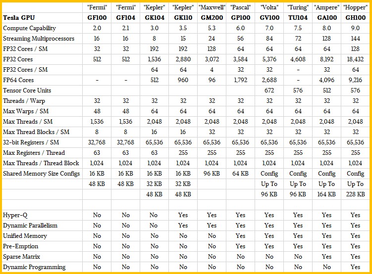
The Hopper GH100 GPU has 144 SMs in total, with 128 FP32 cores, 64 FP64 cores, 64 INT32 cores, and four Tensor Cores per SM. Here is what the schematic of the Hopper GH100 looks like, and you will have to click on that image to zoom in on it because it is a monstrous chip at 80 billion transistors:
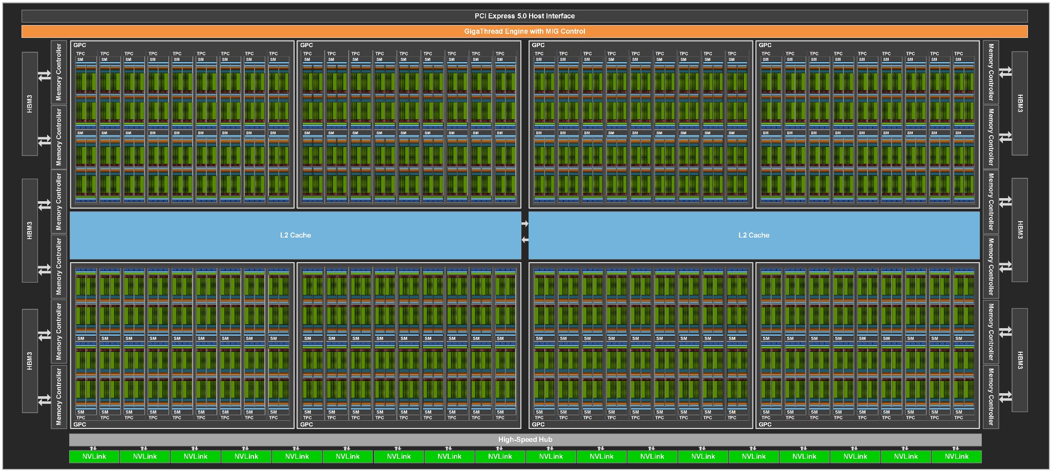
As was the case with the GA100, the GH100 is organized into eight GPU processing clusters, which correspond to the Multi-Instance GPU (MIG) partitions that the GH100 can be carved up into and virtualized – now with full isolation. The GPCs have nine Texture Processing Structures (TPCs), each comprised of two SMs. On the top of the chip is the uber-scheduler, the GigaThread Engine, as well as a PCI-Express 5.0 hos interface. The four of the GPCs are lined to a bank of L2 cache, and there are two banks with a total of 60 MB of capacity.
Along the sides of the GA100 GPU there are a dozen 512-bit memory controllers, which feed out to six HBM3 memory banks. And along the bottom is a high speed hub that all of the GPCs are linked to and that feed out to 18 NVLink 4.0 ports, which have a combined bandwidth of 900 GB/sec.
To get respectable yields, Nvidia is only selling H100s that have different ratios of compute activated, as is common with compute engines. With the H100 in the SXM5 form factor, all eight of the GPCs are active but only 132 out of the 144 SMs are active and only five out of six of the HBM3 memory banks and associated memory controllers are working. So 12.5 percent of the GH100’s compute capacity and 16.7 percent of its memory capacity and bandwidth are dark – the same ratios that were dudded on the GA100 GPU from two years ago. With the PCI-Express 5.0 version of the H100, either seven or eight GPCs are active, and in either case, only 114 of the 144 SMs are active across those GPCs. The same five out of six HBM3 memory banks are active.
Rather than move to chiplets, as Nvidia Research has shown recently that it can do, the GH100 is a monolithic chip in either version.
“We are not adverse to chiplets,” explains Jonah Alben, senior vice president of GPU engineering, referring directly to the co-packaged “Grace” Arm server CPU and the Hopper GPU. “But we are really good at making big dies, and I would say that I think we were actually better with Hopper than we were with Ampere at making a big die. One big die is still the best place to be if you can do it, and I think we know how to do that better than anybody else. So we built Hopper that way.”
The GH100 chip is implemented in a custom variant of Taiwan Semiconductor Manufacturing Co’s 4 nanometer 4N process, and consumes 700 watts in the SXM4 form factor, which is driving memory bandwidth to 3 TB/sec instead of the 2 TB/sec in the PCI-Express 5.0 variant of the card, which weighs in at only 350 watts for nearly the same compute performance. (We will be going over performance, price, and power of the Hopper GPU compared to its predecessors in a separate story, but it is worth point it out briefly here.)
The shrink from 7 nanometer processes used in the Ampere GPU to the 4 nanometer processes used with the Hopper GPU allowed Nvidia to cram more compute units, cache, and I/O onto the die while at the same time raising the clock speed by 30 percent. (The precise clock speeds have not been finalized by Nvidia yet.)
There are a whole bunch of new technologies that enable the Hopper GPU to offer up to 6X more performance than the Ampere GPU it will replace when Hopper starts shipping in the third quarter of this year. We have already talked about dynamic programming and the Transformer Engine acceleration with Ian Buck, who is general manager of hyperscale and HPC at Nvidia. But briefly, the Transformer Engine can selectively apply the new 8-bit FP8 data format to machine learning training or inference workloads and also invoke other reduced precision to speed up transformer neural network models. Importantly, this adaptive precision is dynamically adjusted, based on lots of simulating done on the Selene supercomputer, to maintain accuracy while trying to boost performance to the largest possible extent.
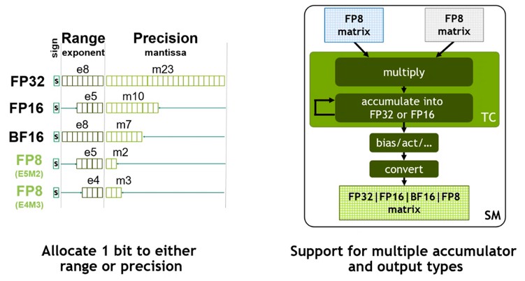
There are actually two FP8 formats in the Hopper GPU: One that maintains the same numerical range as FP16, but has substantially reduced precision, and one that has slightly higher precision but a smaller numerical range. The FP8 matrix math in the Tensor Core can accumulate into FP16 or FP32 formats, and depending on the bias in the neural network, the output can be converted to FP8, BF16, FP16, or FP32 formats.
When you add it all up, the move to the 4 nanometer process allowed the GH100 clock speed to increase by 1.3X and the number of SMs to increase by 1.2X. The new Tensor Core and the new FP32 and FP64 vector units all provide 2X performance boost per clock compared to those in the GA100, and for transformer models, the Transformer Engine with its FP8 precision boosts machine learning throughput by another 2X. That works out to 3X more performance on the vector engines commonly used for HPC and 6X more performance for the Tensor Core engines commonly used in AI.


In Table Turing Compute capability is wrong. It should be 7.5