
As we have seen with various kinds of high bandwidth, stacked DRAM memory to compute engines in the past decade, just adding this wide, fast, and expensive memory to a compute engine can radically improve the effective performance of the device. For some applications, particularly certain kinds of HPC simulation and modeling and certainly for AI training, the higher cost of the stacked memory is the price you have to pay to drive closer to peak performance.
There is nothing easy about making stacked memory, and Micron Technology knows this full well, having started with Memory Cube DRAM a decade ago, which was commercialized in Intel’s ill-fated “Knights” family of Xeon Phi many core processors, and shifted to the High Bandwidth Memory (HBM) standard used by everyone else (including Intel now in its Max Series CPUs, Agilex FPGAs, and Gaudi AI accelerators). But HBM memory needs suppliers beyond SK Hynix and Samsung, and markets tend to like at least three suppliers. And so there is room for Micron, which is looking for something else to sell after the failure of its 3D XPoint ReRAM memory partnership with Intel – a failure due entirely to Intel as far as we are concerned.
Back in June, Micron announced a 96 GB DDR5 registered DIMMs for servers based on its 1α (that’s 1-alpha) process node to make 24 Gb monolithic DRAM chips, which means chips do not have to be stacked to boost DIMM capacity. These 96 GB DDR5 memory modules run at 4.8 GHz and have twice the bandwidth of comparable DDR4 memory DIMMs. (These DDR5 memory modules were tested on “Genoa” AMD Epyc servers using the STREAM Triad benchmark and delivered 378 GB/sec per socket compared to prior the generation DDR4 memory running at 3.2 GHz attached to “Milan” Epyc 7003 series processors, which delivered 189 GB/sec per socket.
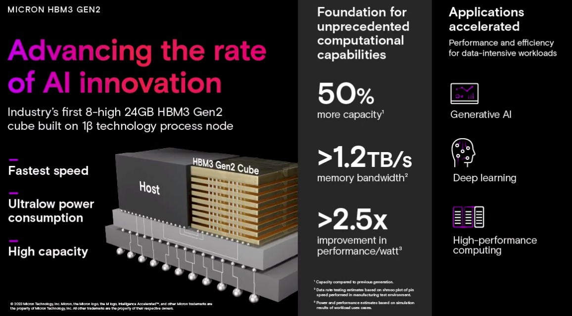
Now, Micron is pushing put its tweaked 1β (that’s 1-beta) process node on etching 24 Gb DDR5 DRAM chips and is embedding them in HBM3 memory stacks in an effort to take on SK Hynix and Samsung. The pin speed on this revved HBM3 Gen2 memory from Micron is 9.2 Gb/sec, which means that an eight-high stack can deliver 24 GB of capacity and 1.2 TB/sec of bandwidth. Which means, in theory, that a device wrapped with eight of these stacks (as is commonly done with Nvidia and AMD GPUs, among other devices) could have a whopping 10 TB/sec of bandwidth – that’s 3.3X what Nvidia is delivering with its “Hopper” H100 GPU accelerator right now – and a very nice 192 GB of capacity – which is 2.4X what Hopper offers.
Most AI shops would take this memory upgrade right now, and gladly pay for it. If they could get a GPU to wrap it around, that is. Micron estimates that using its HBM3 Gen2 memory, existing compute engines could reduce the training time for large language models by 30 percent and would also allow for the number of query inferences per day on these compute engines to be increased by 50 percent. And Micron does this funny piece of math: For an installed base of 10 million GPUs, every five watts of power saved per HBM stack saves up to $550 million in operational expenses over five years.
Micron says that its HBM3 Gen2 memory delivers 50 percent more performance and 50 percent higher memory density compared to currently shipping HBM3 memory, and that its HBM3 Gen2 offers 2.5X better performance per watt than its prior generation HBM2 memory.
The HBM3 Gen2 memory is sampling now, and in the first quarter of 2024, Micron says it plans to start sampling a twelve-high stack with 36 GB of capacity per stack to push the capacity even further.
Micron adds that it has a 32 Gb monolithic DRAM die in the works based on the 1β process that will ship in the first half of 2024 and that will allow it to make 128 GB DDR5 memory sticks, which is more normal sounding capacity than 96 GB to most system architects.

Micron Gears Up For Its Potential Datacenter Memory Boom
If you don’t like gut-wrenching, hair-raising, white-knuckling boom bust cycles, then do not go into the memory business. There is a reason that Intel was driven out of it back in the 1980s, and once again in recent years as it exited the 3D XPoint ReRAM flash-ish memory business. The …

How MCR Memory Can More Than Double HPC And AI Performance
Intel recently demonstrated a new type of DIMM memory technology called Multiplexer Combined Rank (MCR), also referred to as MRDIMMs, that provides up to 2.3X better performance for HPC workloads and up to a 2X better on AI inference workloads in comparison to 5th Gen Intel Xeon processors, based on …
The HBM3 Roadmap Is Just Getting Started
To a certain extent, the only thing that really matters in a computing system is what changes in its memory, and to that extent, this is what makes computers like us. All of the computing capacity in the world, or the type of manipulation or transformation of that data, doesn’t …
HBM is so incredibly wide at 1024 bits of data per stack, and so 1 KB for eight stacks (mentioned in the article). In HBM3 it is split into four 32-bit pseudo-channels per die, so an 8-die stack has 32 of these pseudo channels, and an eight-stack group has 256. This suggests to me that HBM3 can read from 256 different sets of memory locations, over its 8-beat access sequence, getting 32 bytes from each, for further processing (maybe 128 locations for CPUs with 64-byte cache lines, vs GPU’s 32).
If that is correct, then it is quite awesome, and no wonder that memory is so expensive (and something for Micron to also produce). HBM2 had half the channels of HBM3, and HBM had half those of HBM2, so “random (sparse) access” perf should certainly increase with each gen (on top of raised clocks).
I have wondered for a while how many watts these things actually use. So if this single chiplet is running at a full speed of 1.2 TB/s how many watts does it consume?
There’s a ETH Zurich paper by Salami and others (2021, Power Consumption and Reliability of High-Bandwidth Memory) where they state 7 pJ/bit for HBM and 25 pJ/bit for DDRx. Theoretically then, you could transfer 3.5x as many bits per second through HBM and get the same power consumption as DDRx.
Pulled out me quantum computer to slice through the Salami figures … HBM = 1.2 TB/s * 8 bit/B * 7 pJ/bit = 67 Watts. DDRx = 1.2 TB/s * 8 bit/B * 25 pJ/bit = 235 Watts.
I am wondering how HBM3 compare to LPDDR5x / LPDDR6 in terms of 1. Power consumption and 2. Cost (how many times more expensive it is at same capacity) ?
The reason of that is, if HBM3 is much more power efficient, I am wondering why Apple is not attempting to use it in its Pro devices (Mac Pro, Macbook Pro, iPad Pro, iPhone Pro…) ?
I am also wondering how HBM memory stacks power consumption per bit in reading and writing compare to emerging non volatile memory MRAM like Everspin 1Gbit STT-MRAM or European research center IMEC VG-SOT-MRAM, and maybe future VCMA-MRAM ?
The goal would be to get a Non-Volatile Memory (NVM) HBM MRAM stack that is at the same time much, much lower power (at least 1000x) to current HBM stacks : it would be quite disruptive !!!