

While a lot of people focus on the floating point and integer processing architectures of various kinds of compute engines, we are spending more and more of our time looking at memory hierarchies and interconnect hierarchies. And that is because compute is easy, and data movement and memory are getting harder and harder.
To put some simple numbers on this: Over the past two decades, CPU and then GPU compute capacity has increased by a factor of 90,000X, but DRAM memory bandwidth has only increased by 30X and interconnect bandwidth has also only increased by 30X. We have gotten better in some ways in recent years, but we think that the compute-memory balance is still far out if whack, and it means we are overspending on under-memoried compute engines for a lot of AI and HPC workloads.
It is with this in mind that we consider the architectural innovations at the physical layer, or PHY, in networks that have been created by Eliyan and that are being cast in a different and very useful light this week at the MemCon 2024 conference. Co-founder and chief executive officer Ramin Farjadrad took some time to show us how the NuLink PHY and its use cases have evolved over time, and how they can be used to build better, cheaper, and more powerful compute engines than can be done with current packaging techniques based on silicon interposers.
A PHY is a physical network transport device that links a switch chip, a network inferface, or any number of other kinds of interfaces on or within a compute engine to the physical media – copper wires, optical fibers, radio signals – that in turn connects them to each other or to a network.
A silicon interposer is the special circuitry bridge that is used to connect HBM stacked DRAM memory to compute engines such as GPUs and custom ASICs that are commonly used in bandwidth sensitive applications in the HPC and AI arenas. Sometimes HBM is used regular CPUs that are also in need of memory with high bandwidth.
Eliyan was founded in 2021 in San Jose and has grown to 60 people. The company has just taken down its second round of funding for $60 million, with memory maker Samsung and Tiger Global Capital leading the Series B round. Eliyan raised $40 million in its Series A round in November 2022, led by Tracker Capital Management with contributions from Celesta Capital, Intel, Marvell, and memory maker Micron Technology.
Farjadrad cut his teeth as a design engineer at Sun Microsystems and LSI Logic during the Dot Com Boom, was a switch ASIC chief engineer and co-founder at Velio Communications (now part of LSI Logic), and was a co-founder and chief technology officer at Aquantia, which made Ethernet PHYs for the car market. In September 2019, Marvell acquired Aquantia and put Farjadrad in charge of networking and automotive PHYs. Marvell has become one of the largest makers of PHYs, and competes against the likes of Broadcom, Alphawave Semi, Nvidia, Intel, Synopsis, Cadence, and now Eliyan in designing these key components of systems.
Eliyan’s other co-founders include Syrus Ziai, who is head of engineering and operations and who has been vice president of engineering at Ikanos, Qualcomm. PsiQuantum, and Nuvia over the years, and Patrick Soheili, who is head of business and corporate development and who was previously in charge of product management and head of AI strategy for eSilicon. This company is famous for creating the ASICs inside of Apple’s iPod music player and for developing 2.5D ASIC packaging and HBM memory controllers. And of course, eSilicon was acquired by Inphi in late 2019 for $213 million, broadening its PHY capabilities, and in April 2021 Marvell completed the circle by acquiring Inphi in October 2020 for $10 billion.
There is money is PHYs as well as in I/O SerDes and retimers. A SerDes, like those used in switch ASICs to convert parallel data coming out of a device to serial data pumped down a wire or a fiber or over the air, is a special kind of PHY, and to a certain way of thinking, so is a retimer, which will be increasingly used as bandwidth goes up and the length of a copper wire that can push a clean signal consequently goes down.
Fee PHY Faux Big Sum, we say. With that, let’s talk about 2.5D packaging for a minute.
Get Out Your 2.5D Glasses
As Moore’s Law increases in transistor density have slowed and the cost of transistors have come up with each successive process technology rather than going down, we have all been made aware of the reticle limit of modern chip etching processes. With plain vanilla extreme ultraviolet (EUV) water immersion lithography, the maximum size you can etch transistors onto a silicon wafer is 26 millimeters by 33 millimeters.
But many of us are perhaps not aware that is also a limit to the size of the silicon interposer that allows chiplets to be linked to each other on top of the organic substrate that is like a motherboard underneath each compute engine socket and its affiliated HBM memory. The size of that silicon interposer depends on the technology that is used to create the middleboard. (Well, that is what it is.) The interposers are made using the same lithography processes as chips are, but instead of having a reticle limit of 858 mm2 as the chip has, the interposer can be 2,500 mm2 today using some techniques, and closer to 1,900 mm2 using others; there are plans to push that up to 3,300 mm2 according to Farjadrad. Organic substrate sockets do not have such areal limitations. And this is important when you talk about 2.5D packaging of chiplets.
Farjadrad walked us through the feeds, speeds, and limitations of the different 2.5D approaches that Eliyan’s NuLink PHY competes with.
Here is how Taiwan Semiconductor Manufacturing Co does 2.5D with its Chip on Wafer on Silicon (CoWoS) process, which is used to create Nvidia and AMD GPUs and their HBM stacks, among other things:
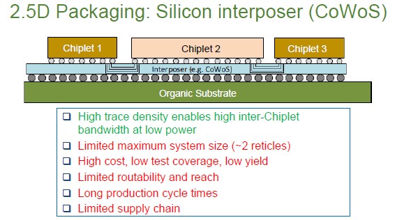
Technically, the chart above shows TSMC’s CoWoS-S interposer technique that is used to link GPUs, CPUs, and other accelerators to HBM memory. The silicon interposer for the predecessor CoWoS-R is limited to about two reticle units – which is exactly the size of the “Blackwell” B100 and B200 GPUs just launched by Nvidia last week, but the that GPU package uses the more modern and less imposing CoWoS-L technique, which is more intricate to manufacture and which is like an embedded bridge used in other approaches. CoWoS-L has a three reticle limit in size.
One bridging technique is called wafer level fan out with embedded bridge, which has been championed by chip packager Amkor Technology and has a variant called FOCoS-B from ASE Holdings. Here are the feeds and speeds for this packaging approach:
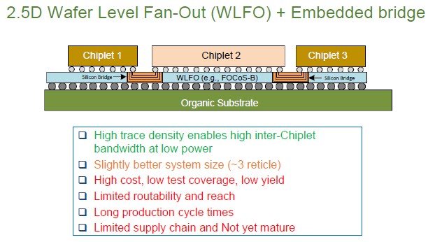
With this kind of 2.5D packaging, you can make a package that is around three reticle limits in size. The high trace wire density means you can get high interchip bandwidth at low power, but the reach is limited and so is the ability to route the traces. Oh, and it has not really be pushed at high volume.
Intel’s approach to putting silicon bridges right into the organic substrate that holds the chiplets – minus an interposer – is similar to what Eliyan is doing with NuLink:
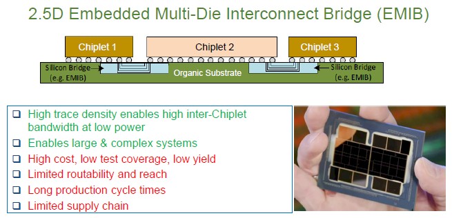
However, EMIB was plagued by long production cycles, low yields, limited reach and routability, and a limited supply chain comprised of one company that does not have a good reputation in advanced semiconductors these days: Intel. To be fair, Intel is getting back on track. But it ain’t there yet.
That leaves the modified 2D MCM process that Eliyan has come up with NuLink:
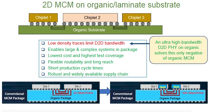 A year ago, the NuLink is PHY had around 10X the data rate of a conventional PHY used in an MCM package, says Farjadrad, and the traces can be 2 cm to 3 cm in length between the NuLink PHYs, which is a 20X to 30X increase over the 0.1 mm trace lengths that are supported by CoWoS and other 2.5D packaging options. That extra distance on the traces, and the fact that the NuLink PHY has bi-directional signaling on those traces, makes all the difference in the world for compute engine design, as you will see. These days there are faster PHYs available for the competition, which has cut that back to a 4X delta.
“With current architectures, when you are running packets of data between the memory and your ASIC, that packet data is not simultaneously bi-directional,” Farjadrad tells The Next Platform. “You either read or write from the memory. If you have a port that can transmit or receive one at the same time, then you can get twice the bandwidth from that same beachfront, which is what NuLink does. You are therefore not wasting half of your ASIC beachfront, which is very precious. We needs our own special protocol to maintain memory coherency, making sure that there is no conflict between reads and the writes. We knew when we made a PHY, and we needed to make an associated protocol for specific applications. This is one of our biggest distinctions. Having the best PHY is one thing, but combining it with the right expertise for the AI application is another important factor, and we know how to do it.”
When NuLink was first introduced back in November 2022, it did not have that name yet and Eliyan had not yet proposed its approach with PHYs to create a Universal Memory Interface, or UMI. NuLink was just a way to implement something that could speak the UCI-Express chiplet interconnect protocol as well as support any protocols that were supported by the original Bunch of Wires (BoW) chiplet interconnect that Farjadrad and his team had created years before and donated to the Open Compute Project as a proposed standard. Here is how Eliyan stacked up NuLink against the various memory and chiplet interconnect protocols:
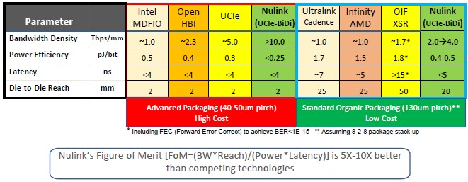
We love this table.
Intel MDFIO is short for Multi-Die Fabric I/O, which is used to connect the four compute chiplets in the “Sapphire Rapids” Xeon SP processors to each other; EMIB is used to link these chiplets to HBM memory stacks for the Max Series CPU variants of Sapphire Rapids that have HBM. OpenHBI is based on the JEDEC HBM3 electrical interconnects and is also an OCP standard. UCI-Express, which we wrote about here, is a funky kind of PCI-Express with the CXL coherency overlay that was designed to be a die-to-die interconnect for chiplets. Nvidia’s NVLink, which it is now using to glue together chiplets on the Blackwell GPU complex, is missing from this table, and so is Intel’s XeLink for its GPU chiplets on the “Ponte Vecchio” Max Series GPU. The NuLink PHY from is, unlike UCI-Express, bi-directional, which means you can have as many or more wires as UCI-Express but double the bandwidth or more across the traces.
As you can see, there is an expensive packaging option that used bumps with a 40 micrometer to 50 micrometer bump pitch, and the die to die reach is only about 2 millimeters. The bandwidth density of the PHYs can be very high – Tb/sec for each millimeter of beach front on the chiplet – and the power efficiency varies depending on the approach. The latency is under 4 nanoseconds across the board as well.
To the right of the table are interconnect PHYs that can work with standard organic substrate packaging and use 130 micrometer bumps, and so are cheaper options. These include the Ultralink PHY from Cadence, the Infinity Fabric PHY from AMD, the OIF Extra Short Reach (XSR) PHY from Alphawave Semi, and the version of NuLink that can still drive pretty high signaling even without resorting to low pitch bumps.
Look at the die-to-die reach on the right side of the table. You can do a lot with 2 centimeters that you just can’t do with 2 millimeters and a 0.1 millimeter spacing between the ASIC and the HBM stack or the adjacent chiplet. These longer links open up the geometries of compute and memory complexes and they also eliminate the thermal crosstalk effects between ASIC and HBM. Stacked memory is very sensitive to heat, and as GPUs have gotten hotter, there is a need to cool the HBM so it works properly. If you can get the HBM further away from the ASIC, you can run that ASIC faster – Farjadrad estimates about 20 percent – and hotter because the memory is not close enough to be directly affected by that increasing ASIC heat.
Moreover, by removing the silicon interposer or equivalents in a device like a GPU and by moving to organic substrates and using fatter bumps and spacing out the components, you can drop the manufacturing cost of a dual ASIC device with a dozen HBM stacks from about $12,000 with a chip plus package yield of around 50 percent to a device with an 87 percent yield at cost of around $6,800.
Let’s look at two more charts contrasting UCI-Express, BoW, and UMI and then we can play system architect for a bit.
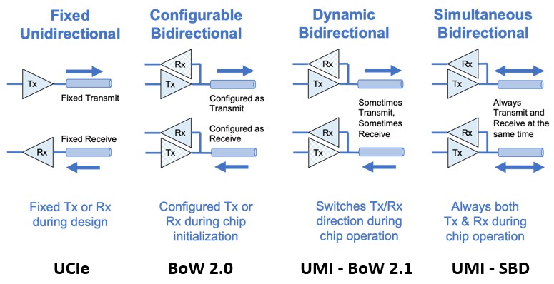
As you can see, Eliyan has kept pushing the envelope on the bi-directional capabilities of its PHYs, and now has the ability to do simultaneous bi-directional traffic, which it is calling UMI-SBD.
And here is one that shows the bandwidths and ASIC beachfronts for these same four options:
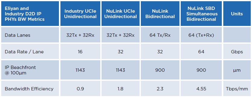
So the NuLink PHY, which is now being branded as UMI, is smaller, faster, and can pitch and catch at the same time than UCI-Express. What can you do with it?
First, you can build bigger compute engines:
How does 24 or more HBM stacks and a compute engine package of between 10 and 12 reticals grab you? And that is a device that takes one-quarter to one-fifth the time to manufacture because it is on standard organic substrates.
There was a saying that was once pegged to IBM in the early 1990s after it started falling from its peak in 1989 or so: You can find better, but you can’t pay more.
Nvidia is no IBM, of course. Or Intel. Not yet, anyway. Easy money does weird things to companies and their roadmaps.
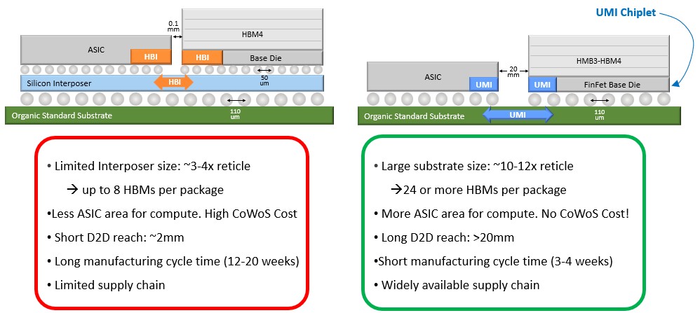
Here is how Eliyan thinks HBM4 might play out in the future:
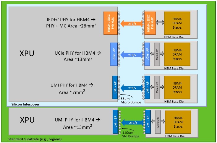
The JEDEC PHY for HBM4 memory is a fatty, and switching to UCI-Express will cut that area in half. Using the NuLink UMI PHY will almost cut it in half again, leaving that much more room for logic on the XPU of your choice. Or, if you want to ditch the interposer, make a much, much larger device, and put up with a 13 mm2 UMI PHY, you can build a much cheaper device, too, and still drive 2 TB/sec out of each HBM4 stack.
Now here is where it gets interesting.
Back in November 2022, when Eliyan was pitching its ideas, it was comparing a GPU with an interposer linking to its HBM memory with a beast of a machine that removed the interposer and doubled up the ASICs (much as Blackwell has done) and put a wonderful 24 HBM ranks against those ASIC chiplets. Like this:
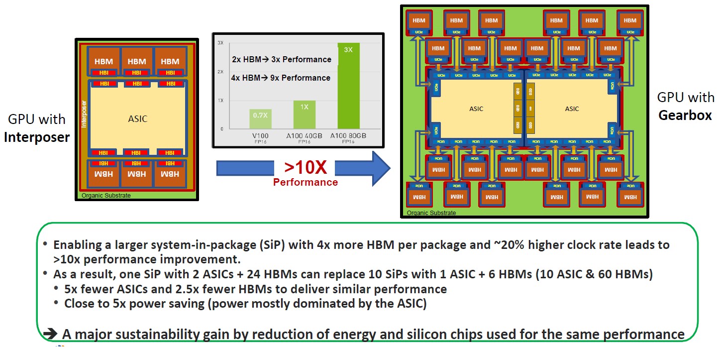
On the left is how the Nvidia A100 and H100 GPUs and their HBM memories are architected. And in the middle is an Nvidia chart that shows how performance goes up as more HBM memory capacity and more HBM memory bandwidth is made available to AI applications. And as we know, the H200 with 141 GB of HBM3E memory and 4.8 TB/sec of bandwidth does 1.6X to 1.9X the work of an H100 with the same exact GH100 GPU but with only 80 GB of HBM3 memory 3.35 TB/sec of bandwidth.
Imagine a beast as shown above with 576 GB of HBM3E memory and 19 TB/sec of bandwidth! Remember: The memory is not a huge part of the power draw, the GPU is, and the little evidence we have seen to date surely indicates that the GPUs being put into the field by Nvidia, AMD, and Intel are all constricted on HBM memory capacity and bandwidth – and have been for a long time because of the difficulty in making this stacked memory. These companies make GPUs, not memory, and they maximize their revenues and profits by giving as little HBM memory as possible against formidable amounts of compute. They always show more than the last generation, but the GPU compute always goes up faster than the memory capacity and bandwidth. Such as design as Eliyan is proposing can snap the compute and memory back into balance – and make these devices cheaper, too.
Perhaps that was a bit too strong for the GPU makers, so with the UMI launch, the company has backed off a little and showed how a mix of interposers and organic substrates plus the NuLink PHYs might be used to make a larger and more balanced Blackwell GPU complex.
Below on the left is how you would create a Blackwell-Blackwell superchip with a single NVLink port running at 1.8 TB/sec linking the two dual-chiplet Blackwell GPUs together:
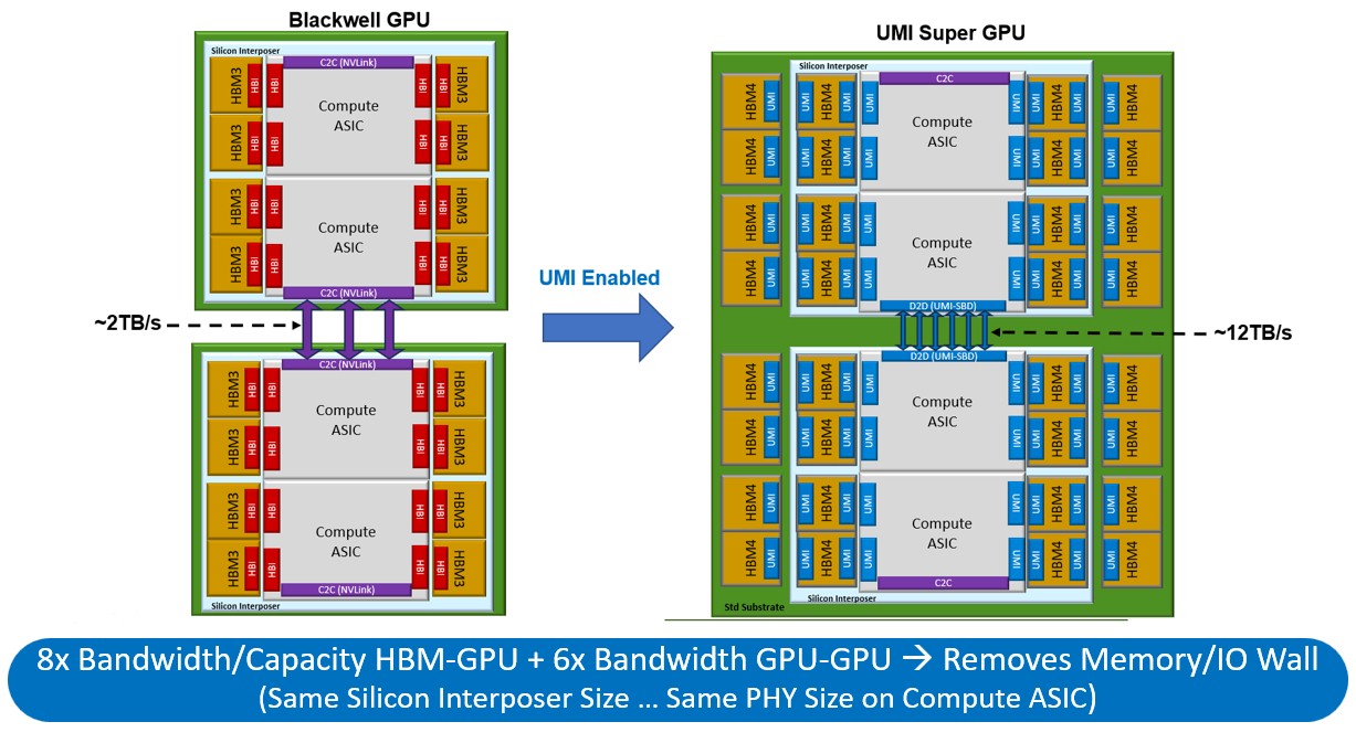
With the NuLink UMI approach, which you see on the right in the chart above, there are six ports that deliver around 12 TB/sec of bandwidth between the two Blackwell GPUs – a little bit more than the 10 TB/sec that Nvidia is delivering with NVLink ports that zipper the two Blackwell dies together in the B100 and B200. That is 6X the bandwidth in the Eliyan superchip design than in what will likely be the Nvidia B200 superchip design, if it has one. Eliyan can put the same eight banks of HBM3E memory on the interposer if Nvidia wants to stick with its CoWoS manufacturing process, but it can then put another eight banks of HBM3E onto each Blackwell device, for a total of 32 banks of HBM3E, which would yield 768 GB of capacity and 25 TB/sec of bandwidth.
Just chew on that for a second.
But wait, that’s not all you get. This UMI approach works for any XPU and it works for any kind of memory, and you can do crazy things like this, all on a massive organic substrate and without the need for interposers:
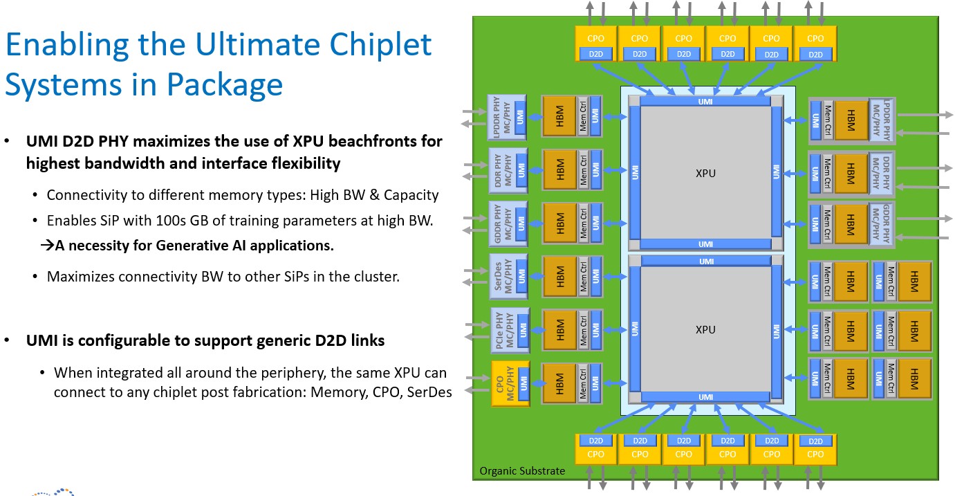
Any memory, any co-packaged optics, any PCI-Express or other controller, can be linked using NuLink to any XPU. At this point, the socket really has become the motherboard.
And for even larger complexes, Eliyan can build NuLink Switch. . . .


Hi Timothy,
NuLink sounds impressive and makes sense if I follow the arguments correctly. But has Eliyan produced any hardware to verify and validate this yet?
They have done their PHY in 5 nanometer and 3 nanometer processes as far as I know. And they have one large scale customer, someone not quite a hyperscaler but more than a typical service provider.
So if I’m reading this article correctly and especially the viewpoint stated that the socket is becoming the motherboard, could we begin to see by the end of this decade the socket growing so large as to begin looking like Cerebras’s wafer scale chip ?
But made of chiplets with interconnects.
So the socket will TRULY be the motherboard. I’m actually starting to believe this to be true . I mean, extrapolate this out. Does a desktop AI PC in 2035 ( whatever that means in 2035 much less today ) have a motherboard with nothing but one huge socket and traces on the motherboard for various physical connections like USB, HDMI, and Ethernet? Could you see a NUC sized mini PC where the motherboard is only as large as the socket itself as there is no need for any external connectors as everything is wireless in and out? Or another extreme. What happens to the Raspberry Pi when the socket becomes bigger than today’s motherboard? Will that become the ultimate expression of an SBC when quite literally the socket is the single board and the computer simultaneously?
I think so.
I’m not sure whether to be amazed or frightened. I remember the day hawking 3rd party modem cards and convincing folks to go with brands that had the Lucent 56k chip as opposed to the Rockwell chip. Then suddenly….poof….supply dried up as everything started going into the motherboard. It’s like I’m the silicon version of a black hole creation . You first see the parent star swell and swell until it explodes, collapses into itself, only to be reborn into something even larger.
I imagine you only use the high performance connect for things that need it. One for cost, but two for reliability. Ideally you don’t rip out all the compute engines and high performance memory because the usb controller died. The more chips you pack onto the device, the more chances there are for one of them to go bad and cause you to throw the whole thing away. Perhaps you build in redundancy and just ignore failures, but that increases complexity, leading to a higher rate of errors, etc.
Interesting! Maybe this NuLink-PHY based UMI (bi-directional, interposer-less, UCIe/BoW-compatible) can be part of the next generation of UCIe (if it gets called UMI-express) — especially as Intel provided Series A funding to Eliyan (with Marvell and Micron, as stated in the article). And with “NuLink Switch” (last sentence) Nvidia competitors could get a few legs up on putting rack-scale units of computing together, that potentially outdo the NVL72 in AI (noting though that Nvidia has some level of “in-switch computing” for hierarchical aggregation, and automated adaptive tensor-block precision in the FP8, FP6, FP4 range).
In particular, bypassing the CoWoS heartburn-indigestion, looks to me like the healthier way to go about HPC/AI/ML gastronomy (if it works right … seeing how the 2D MCM image does look visually like 2.5D EMIB). This could be a winning tech from Eliyan.