

We don’t like a mystery and we particularly don’t like it when what is very likely the most powerful supercomputer in the world – at this time anyway – is veiled in secrecy. But that is what the Tianhe-3 supercomputer built for the National Supercomputer Center in Guangzhou, China has been. Everyone has been trying to suss out what this system might look like. And the usual suspects here in the United States who would normally know, don’t.
So we are going to take a stab at figuring out what Tianhe-3 might look like. Just like we did for the “Oceanlight” system installed at the National Supercomputer Center in Wuxi, China before some details of the machine were disclosed thanks to the Gordon Bell Prizes that this particular beast has won.
Both the Oceanlight system and the Tianhe-3 machine, which very likely has the nickname “Xingyi” based on recent reports coming out of the Middle Kingdom, are too important to ignore. And we need to not only understand these two machines ahead of the formal disclosure of the capabilities of the “El Capitan” supercomputer being built right now at Lawrence Livermore National Laboratory by Hewlett Packard Enterprise in conjunction with compute engine supplier AMD. We need to know because we want to understand the very different – and yet, in some ways similar – architectural path that China seems to have taken with the Xingyi architecture to break through the exascale barrier.
Just because the details of these machines in their fullest configurations have not been disclosed by the Chinese government does not mean they do not loom large over the upper echelons of supercomputing.
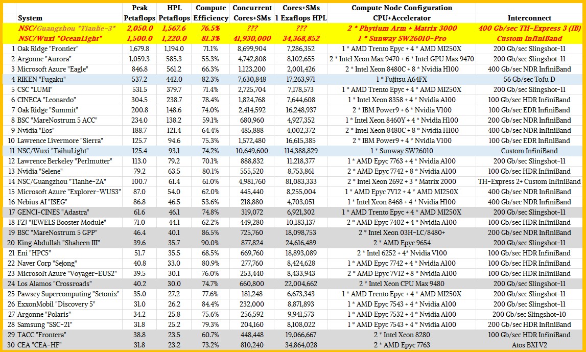
That is why in our analysis of the Top500 supercomputer rankings back in November, we reminded everyone that based on the rumored performance of Xingyi at NSC Guangzhou – 2.05 exaflops peak and 1.57 exaflops sustained on High Performance LINPACK – that it was the most powerful machine yet assembled on Earth. And we also reminded everyone that the Oceanlight system at NSC Wuxi was the second most powerful machine on the planet, with 1.5 exaflops peak and around 1.22 exaflops sustained on LINPACK. So this is how the actual Top30 supercomputer rankings in November might have looked had China submitted results:
We think there is a very good chance that El Capitan will come in at 2.3 exaflops peak when it is fully fired up, hopefully by the June 2024 rankings. You can bet Elon Musk’s last dollar that the premiere supercomputing lab in the United States will be getting all the help it needs to beat what we think the two Chinese machines can do.
An Evolutionary Approach
There have been five Tianhe machines built in China (six if you count the Tianhe-3 prototype), all of them designed and constructed by the National University of Defense Technology. (Tianhe is Chinese for “Sky River” and refers to what we in North American and Europe call “Milky Way” after the edge of our galaxy that we can see spanning the night sky.) And as you can see, the third machine, Tianhe-2A, is still powerful enough to make the Top30 rankings of real supercomputers even after being in the field for a long time.
Tianhe-1 was revealed in October 2009, and was ranked fifth on the Top500 list that fall. Tianhe-1 had a hybrid CPU-GPU architecture, which was just starting to become more commonplace at the time, and used 5,120 Intel Xeon E5 processors that were paired 1:1 with 5,120 AMD GPU. There were 2,560 two-socket Xeons server nodes with an equal number of dual Radeon 4870 X2 cards. This machine had 1.2 petaflops peak and 563 teraflops of LINPACK oomph. This machine was installed at the National Supercomputer Center in Tianjin, China. (Which is why our original Top500 chart back in November placed Tianhe-3 there incorrectly.)
A year later, the Tianhe-1A machine was launched, and not only did it have lot more 64-bit floating point oomph and a different architecture, it was the highest performing machine that China had ever built. This machine had 7,168 two-socket Xeon X5670 server nodes, each one with an Nvidia M2050 GPU. There were an additional 2,048 FeiTeng 1000 Sparc T5 clones – the T5 design was open sourced by Sun Microsystems – that were part of the Tianhe-1A system, but they did not underpin the LINPACK results. This system had 4.7 petaflops of peak performance and 2.57 petaflops sustained on LINPACK, and really marked the rise of China in HPC. Tianhe-1A was noteworthy in that it also included a proprietary interconnect code-named Arch that ran at 160 Gb/sec and that we still believe, based on rumors, was an overclocked or enfattened variation of QDR InfiniBand. This interconnect has evolved and is now called TH-Express as far as we know.
At the time, there was talk that the next-generation Tianhe machine would be based on the homegrown Loongson MIPS architecture and would be designed and built by upstart Chinese server maker Dawning. But that didn’t happen.
With the Tianhe-2 machine, NUDT was able to get the machine into the field two years early and moved the family of hybrid supercomputers to NSC Guangzhou in the southern part of China for reasons that have never been explained but were probably political in nature. One reason it could be fast is that it was based on Intel Xeon CPU and “Knights” Xeon Phi manycore accelerators. To be precise, Tianhe-2 had 16,000 nodes, each with a pair of Xeon E5-2692 processors and four Xeon Phi 31S1P accelerators. It cost around $390 million to build, and was twice as fast as the “Titan” supercomputer at Oak Ridge National Laboratory when it came online in 2013. Tianhe-2 was rated at 54.9 petaflops peak and 33.9 petaflops sustained on LINPACK, a 62 percent computational efficiency that was a lot better than the 47 percent that NUDT got with the Tianhe-1A system. Tianhe-2 did burn 17 megawatts, though.
Soon after Tianhe-2 was in the field and as Intel was ramping up the Knights family of accelerators, the US government decided to ban the importing of these Xeon Phi chips to China in an effort to curtail its advances in nuclear weapons and aircraft design, among other things. And so NUDT got to work on building its own floating point accelerators, in this case not based on X86 cores with fat vector engines but on DSPs designed to do matrix math.
The architecture of NUDT’s Matrix-2000 DSP accelerator was unveiled in July 2015 at the ISC supercomputing conference; some feeds and speeds of the Tianhe-2A machine that would use it instead of Xeon Phi coprocessors were revealed in September 2017 and more details about the system were divulged in February 2018 as it was being installed in time for June 108 Top500 rankings, where it ranked fourth place. The system design stayed essentially the same, with one two-socket Xeon E5 node having four Matrix-2000 accelerators, which are also known as the MT2000s. Tianhe-2A’s node count went up to 17,792, and that plus the use of the Matrix-2000s pushed the peak theoretical performance of the machine up to just a tad under 95 petaflops peak. The machine has been expanded a bit since its initial installation and is now rated at 100.7 petaflops peak and delivers 61.4 petaflops sustained LINPACK, which is a 61 percent computational efficiency. That’s not great, but it is acceptable if that is all you can do and you need to get some HPC and AI done. The “Galaxy” interconnect signaling for Tianhe-2A was boosted to 14 Gb/sec from the 10 Gb/sec used with the Arch interconnect used in Tianhe-1A and Tianhe-2, and presumable the bandwidth per port was raised from 160 Gb/sec to 224 Gb/sec.
We caught wind of the Tianhe-3 prototype system as it was being tested running AI networks in this paper (which was gated), and we covered the architecture of compute elements in the Tianhe-3 machine here. That would be the Phytium Arm CPU, called the FT-2000+, and the updated Matrix-2000+ DSP accelerator, which is also known as the MT-2000+ depending on where you look. That paper included a sketch of the processor, which is visible through Google search despite the paywall:
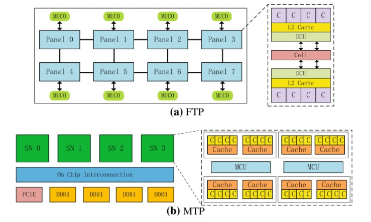
The Phytium Arm core complexes are on top and the Matrix core complexes are on the bottom and that picture sure does seem to imply that the Tianhe-3 architecture would have two discrete devices as the four prior production Tianhe machines deployed (and possibly the Tianhe-3 prototype). Don’t quite jump to that conclusion yet.
On the CPU side of the Tianhe-3 prototype, the core complexes have 32 KB of L1 cache per core and share 2 MB of L2 cache for each quad of cores. These quads are interconnected to share their memories very fast. Eight of these core complexes are connected in a mesh, and all of the cores run at 2.2 GHz and provide 614.4 gigaflops of FP64 performance.
The MT-2000+ part of the Tianhe-3 prototype has a hierarchical compute and memory fabric as well, with four super nodes, or SNs that are themselves comprised of eight DSP core and cache complexes with memory control units linking them all to each other. The DSP super nodes are interlinked with an on-chip interconnect that supposedly runs at 200 Gb/sec bi-directionally. (This seems way to slow. We would expect something more like 2 Tb/sec.) You will note that there are four DDR4 memory controllers and one PCI-Express controllers hanging off this on-chip interconnect. As far as we know, performance metrics for the Matrix-2000+ accelerator were not divulged.
That brings us – finally – to Xingyi, or Tianhe-3, if we are understanding the codename correctly. Here is a short video that China Central Television put out about the new machine when it was unveiled on December 6, and here is a report from Sina Technology on the same day.
We usually only poke around when we are suspicious or bored, and so we missed it when a case study on programming the Matrix-3000 accelerators was submitted to arXiv on October 21, 2022. It is called Programming Bare-Metal Accelerators with Heterogeneous Threading Models: A Case Study of Matrix-3000, and you can download it here. There is also another paper that talks about the Matrix-3000 called MT-3000: A Heterogeneous Multi-Zone Processor For HPC, which is behind a paywall here and which was published in May 2022.
The abstract for this latter paper behind the payroll lays a lot of it out for all of us to read if you only know to search for “MT-3000” instead of “Matrix-3000,” which is funny. In any event, here is what it says right up front:
“With high performance computing (HPC) continues evolving, high performance microprocessor, which is the key building block of super computer, becomes the jewel in the crown of HPC. To this end, we propose MT-3000, a heterogeneous multi-zone processor for HPC, which is entirely designed and implemented by National University of Defense Technology. MT-3000 contains 16 general purpose CPUs, 96 control cores and 1,536 accelerator cores, which are grouped into a general purpose zone and an acceleration zone. The acceleration zone is further divided into four clusters. Through sophisticated designs of such multi-zone organization, interconnection, and memory subsystem, MT-3000 achieves 11.6 teraflops double precision performance and 45.4 gigaflops/watt power efficiency when operating at 1.2 GHz. Based on the MT-3000 chip, a supercomputer prototype with nearly 12 petaflops peak performance is implemented, achieving 80 percent computation efficiency for LINPACK. The possibility of a larger scale supercomputer construction based on MT-3000 chip is also elaborated in this paper.”
No kidding.
This MT-3000 is not an accelerator, but a hybrid device with CPU and accelerator compute as well as three different kinds of memory, two of which are located in the compute complex. So it is akin to the AMD “Antares” MI300A CPU-GPU hybrid that is going into El Capitan than it is like the discrete CPU-GPU systems we see pushing the flops in AI and HPC systems these days. The MT-3000 is its own animal, and you might assume that it uses a chiplet packaging architecture given that Semiconductor Manufacturing International Corp (SMIC), the indigenous Chinese foundry, probably could not cram enough transistors into a 14 nanometer process to make a monolithic die. But, then again, maybe this is a 10 nanometer or even a 7 nanometer device. If NUDT doesn’t care about cost, then the yield can be terrible so long as SMIC can find tens of thousands of good MT-3000 parts to make the system.
We would love to learn more. For now, we will tell you what we think we know.
Let’s start with the block diagram of the MT-3000:
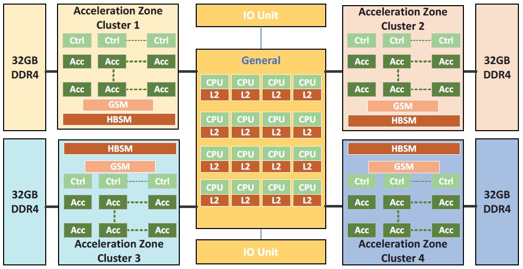
At the heart of the device is not 64 cores like the prototype, but only 16 cores, which we presume are Arm cores, that link out to four DSP acceleration clusters. The two I/O controllers hang off of the CPU complex, which has four accelerator complexes also hanging off the CPUs. You will not that the MT-3000 uses plain old DDR4 main memory to feed into the accelerators, and has only 32 GB per accelerator complex for a total of 128 GB. This MT-3000 was designed maybe four years ago and installed more than two years ago, so that stands to reason. If you are risking with a completely new design idea, you don’t mess around being on the bleeding edge of memory or I/O controllers.
The general purpose zone, as NUDT calls the central CPU complex, runs at 2 GHz, while the acceleration zone, which is divided into four acceleration clusters, runs at 1.2 GHz and delivers that 11.6 teraflops at double precision according to both papers. That 45.4 gigaflops per watt of computational thermal efficiency means it runs at around 256 watts, and presumably that includes everything but memory. Maybe it even includes that, which might be less than 40 watts. Assume not and call it 300 watts for the complex including memory. That’s our hunch.
And if we are right, that is almost precisely the spec of the “Arcturus” Instinct MI100 GPU accelerator. Which was rated at 11.5 teraflops at FP64 precision in 300 watts.
Looking at the cores for a second, and assuming this is just a Phytium FT-1000 chunk running at 2 GHz instead of 2.2 GHz as in the prototype for Tianhe-3 and assuming it was the same Arm core, then this CPU complex should deliver about 140 gigaflops of FP64 oomph itself. But that’s not its purpose. The GP zone runs a Linux operating system as a host of the four accelerator complexes, which do not have an operating system.
Each CPU core in the MT-3000 complex has its own L1 and L2 cache. We assume the L1 cache is still 64 KB and we know that the L2 cache has stayed at 512 KB – the same ratio as used in the prototype per core. But now, each L2 cache is dedicated to each core, it is not a 2 MB cache shared across four cores.
Each of those accelerator complexes has 24 control cores and 384 accelerator cores, and because software compatibility is an issue for codes written for the Tianhe-2A machine, we presume these accelerator cores are DSPs that do matrix math in much the same way as the MT-2000 and MT-2000+ discrete accelerators did. (Was there ever an MT-1000 that was designed even before the embargo on Intel stuff hit? Maybe used for military purposes? Hmmmm. . . . )
You will note something else very interesting. The accelerators have two types of on-chip memory: scalar memory (SM) and array memory (AM). The scalar memory buffer is 64 KB and is private to each control core, and the array memory weighs in at 768 KB and is private to a group of 16 DSP cores. And then they also have three types of shared memory: global shared memory (GSM), high bandwidth shared memory (HBSM), and that external DDR4 main memory. The CPUs can access any of the GSM, HBSM, or DDR4 memory, but the accelerators can only access the GSM, HBSM, or DDR4 memory attached to their quarter of the acceleration units. Data transfers between the accelerator quads are managed by the CPUs. The HBSM in each quad is 48 MB with 307 GB/sec of bandwidth, and each 32 GB DDR4 memory block has 204 GB/sec of bandwidth. The GSM is only 6 MB and is like an L3 cache for each accelerator complex.
Here is the layout of the MT-3000 chip, which indeed appears to be monolithic:
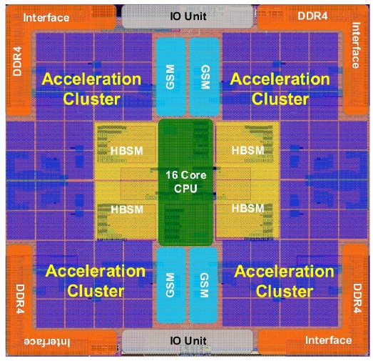
Pretty, isn’t it?
There were apparently two Tianhe-3 prototypes, because there was one using the real MT-3000 that scaled to 1,024 nodes and that delivered 11.88 petaflops of FP64 oomph with a computational efficiency of 82.1 percent on LIPACK, according to the first paper mentioned above. A single MT-3000 device has a computational efficiency of 90.1 percent.
So now, let’s have some fun and build Tianhe-3 in our minds. Just like the first paper did. You start with a blade, which has one MT-3000 hybrid CPU-DSP compute engines. You put 32 of these plus four communication blades (presumably running at 224 Gb/sec using he Galaxy TH-2 interconnect) for a total of 800 Gb/sec of bandwidth, plus two management blades (redundancy is important) and that makes a building block. Eight of those building blocks get loaded front and back in a rack, and eight of those racks make the 11.88 petaflops system. The paper said that NUDT and NSC Guangzhou had extrapolated that a system of 100 cabinets would have around a 75 percent computational efficiency on LINPACK.
Go back up to that big quote above. There is a mistake in it. That 11.6 teraflops rating for the MT-3000 is not peak theoretical performance; it is peak LINPACK performance at 90.12 percent computational efficiency. As is noted elsewhere in the first paper. Which means the peak performance is more like 12.87 teraflops for each MT-3000 device. That distinction is important as we scale up beyond 100,000 devices to make Tianhe-3.
If Tianhe-3 is rated at 1.57 exaflops on LINPACK, if you assume the efficiency is around what the rumors said last year, then 625 cabinets with 160,000 MT-3000s should give you 2.06 exaflops peak and that 1.57 exaflops LINPACK rating. That is 2.56 million Arm cores and 245.76 millions DSP cores.
One last thing: The press reports from December said that the Xingyi system was “double” Tianhe-2A, which would around 200 petaflops peak. We think something got lost in translation there. A 200 petaflops MT-3000 machine would not break any records or shake anything up. Although it would be fun to play with, just the same.
China could just tell us how it built Tianhe-3 and when.


I don’t understand Chinese but isn’t that the Tianhe-3?
https://www.youtube.com/watch?v=8-KLHyTZSlU&ab_channel=%E7%94%B5%E5%AD%90%E6%A2%A6
Some of the presentation might be, but it looks like OceanLight based on the speeds. It is as if we are behind the presentation, which is a neat obfuscation trick.
Superb detective work on Guangzhou’s Xingyi architectural mystery! I like the idea of Tianhe-3 being an MT-3000 affair with ARMs and matrix-dsp combined in-package, as it is reminiscent of Grace-Hopper superchips, and of what Ampere could do by plunking chiplets of its CPU cores, in-package, with some AMD Aqua Vanjarams, for a Poseidon mermaid follow-up to siryn!
The 26x performance jump from Tianhe-2A’s Xeon+Matrix-2000 looks quite large (61 PF/s to 1.57 EF/s) but Riken did recently succeed at a 42x jump between the SPARC64-based K super (2011-2019) and the A64FX-based Fugaku (10.5 PF/s to 442 PF/s) which suggests it is quite possible (both of which beat Italy’s Eni 9x jump with HPC6; France’s Total meanwhile, with record profits, will obviously need to retort in kind, with a 30x upgrade to Pangea III, before too many tourists end-up in the Po River, rather than on the shores of the Seine!).
I wonder if Chinese engineers and scientists have ideas for approaching the flexibilization of interconnects (and distribution of memory), to support reconfigurable dataflow-like operation in such hybrid systems.
I think Nicole and I could use some time by the Seine as well as by the Po! We might need a tour guide, though…. Can you think of anyone?
Ask Microsoft; they probable have a Copilot in Paris. If it doesn’t work, just reboot your vacation.
Chines engineers and scientists do have such ideas.
“China could just tell us how it built Tianhe-3 and when.”
Yeah, more sanctions is always a good thing, right?!
It sure hasn’t stopped them.
How do you know, nobody knows
Sanctions are like boomerangs; throw them, and come back to you.
Excuse total followers HPC news: América dont it have zettaflops machine not by tech lack, America firts goal its efficiency dont mad spendthrift cost of Watts consumption. The planet health its firts priority. !! . !
It’s an easy thing. Just go there and talk to the people. HPC still is open science and there are no real secrets about Tian-He 3 or any other Chinese HPC system.
https://patents.google.com/patent/CN104756078B/zh
I don’t believe ANYTHING at face value coming from the CCP. Just look at their falsified GDP figures over at least the last decade, and the admission they “over counted” their population by 100,000,000. This coming from the party who NEVER admits errors. They’ve simply butchered that many people. China is the most prideful, insecure nation ever. They object to criticism from folks in the Free World, which isn’t their prerogative. Every time a significant technical achievement is announced through peer review, CC propaganda claims they did it first and better. I’ve studied CCP history and polity for over 30 years as a professional analyst. The CCP and any organization in China simply cannot be believed.
How long have you had this symptom? Go to the hospital quickly to see if it can be saved.
of course china would keep it hidden. the new tech created by the rest of the world is either stolen by china or just plain reverse engineered by china. keep new tech away from china, because china will try and take over the planet when they think they can do so.
I believe if budget has no limits, we can build out as large as we want, given the space and power supply. Depends more on priorities, and allocation of tax money of course. Sanctions do come back to bite, and the need for ever increasing compute power, for what ever the reason will continue, even if to be at the top of the chart……. Super supremacy is a big thing. Maybe we should get back to climate change and workout how to fix it.
The Guangzhou machine is not Tianhe-3 (that one is located far north) but 1/10 scale “mini me” version
Its a old RadioShack
Tianhe Xinyi is not Tianhe-3. It’s a more powerful variant of Tianhe-2 and is based in Guangzhou. Read this news https://www.21jingji.com/article/20231207/herald/d5b36913e711818127194826c02fddaf.html
This news report says Tianhe Xingyi’s performance is 5x that of Xinghe-2 and is built to support industrial applications. I find it interesting that the video shows a garment factory using the super computer to manage its inventory. Wow! Who says China is deprived of compute power due to the sanctions?
https://www.youtube.com/watch?v=NmXlJjnx8R0
Can we please stop calling nVidia’s thing a superchip. It is impressive but it is not supernot, especially when compared to AMD’s APU Mi300 thing.
Superchip means a dual-chip module across two sockets. I don’t have a better word for it. And at some point, either others will do this or Nvidia will stop and it becomes a non-problem.
Just call it Grace-Hopper or whatever. If nV had not used the word superchip then it would have had a much harder time grabbing mindshare. Now every fan boie on the planet is running around with “superchip, nV has a super chip”, and the accountants feel better betting money on it relatively untested. It’s the most transparent marketing manipulation-speak by nV. Journos should not play along.