

Heaven forbid that we take a few days of downtime. When we were not looking – and forcing ourselves to not look at any IT news because we have other things going on – that is the moment when Nvidia decides to put out a financial presentation that embeds a new product roadmap within it. Thanks.
The good news is that this new Nvidia chip roadmap, which covers GPUs, GPUs, and switch ASICs, gave us something to talk about as soon as we fired up the trusty keyboard here on Thursday morning. So thanks for that, truly.
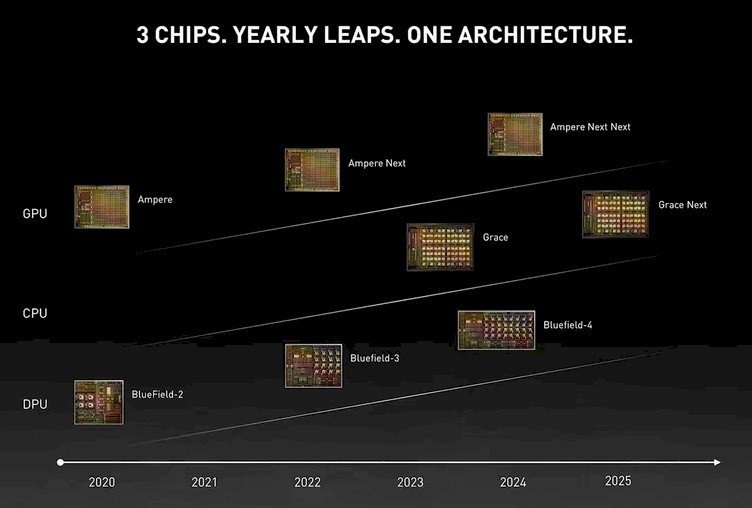
Let’s drive right in, and let’s start by reviewing the roadmaps from the past few years. Here is the one from GTC 2021, which was held in April of that year:
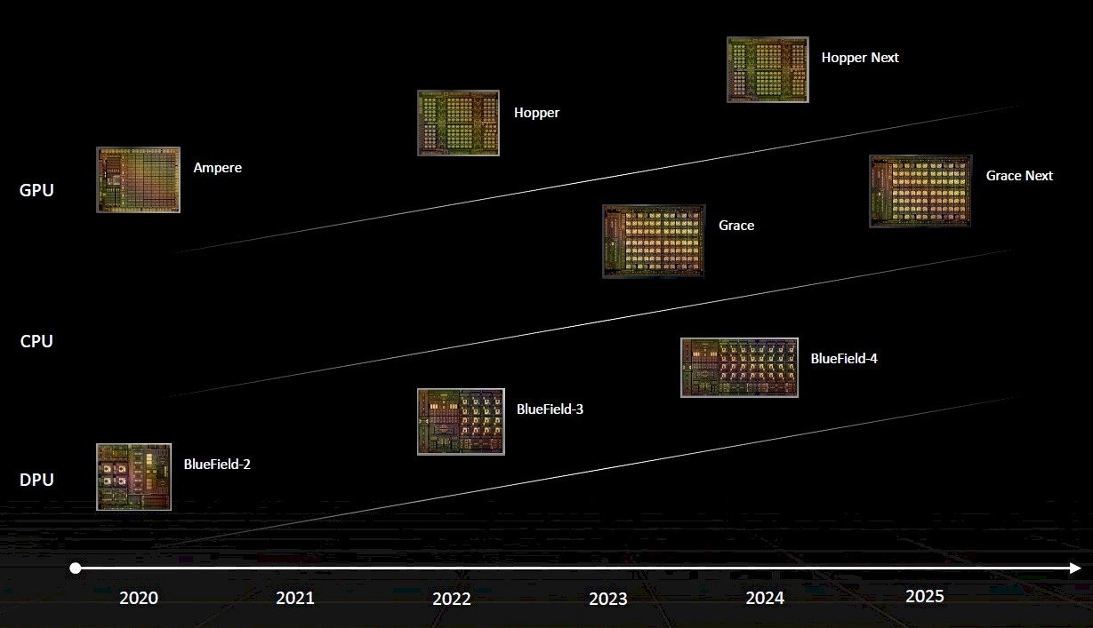
And here is the updated one after “Hopper,” which was called “Ampere Next” in the roadmap above, that came out at Computex 2022:
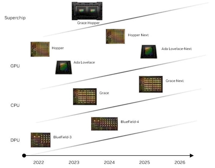
Here is an update to the roadmap that we think came out earlier this year, which added the “Lovelace” line of GPUs that are used in AI inference, visualization, and metaverse processing cards:
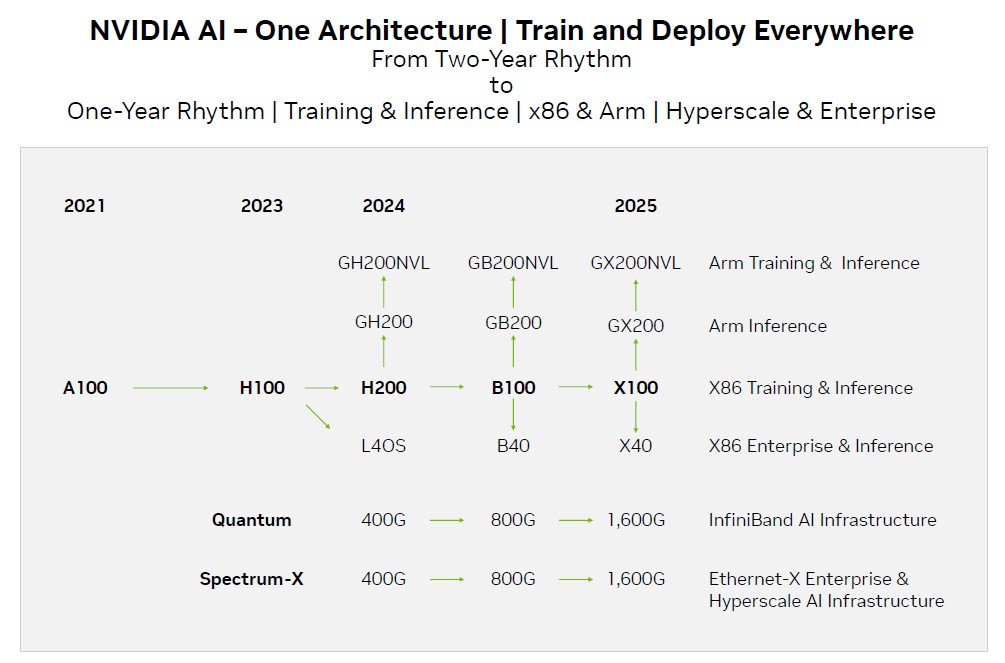
And finally, here is the roadmap that Nvidia just put out sometime in early October that we all just saw:
If past trends are indicators of future trends – and they most certainly are supposed to be when chip makers promise their hyperscaler and cloud builder customers a two-year cadence for launches, as Nvidia did a number of years ago – then we were absolutely expecting a newly architected Blackwell GB100 GPU accelerator sometime around March through May next year. But as you can see below, the cadence of major GPU releases from Nvidia has often been shorter than two years. So this is a kind of return to form.
Here are how the datacenter GPUs rolled out in the past 11 years that datacenter GPU compute mattered:
- “Kepler” K10 and K20, May 2012
- “Kepler” K40, May 2013
- “Kepler” K80, two GK210B GPUs on a single card
- “Maxwell” M40, November 2015, mostly for AI inference not really for HPC or AI training
- “Pascal” GP100, April 2016
- “Volta” GV100, May 2017 (some features of the original Pascal did not make it until Volta)
- “Ampere” GA100, May 2020
- “Hopper” GH100, March 2022
- “Hopper-Next” H200, spring 2024?
- “Blackwell” GB100, summer or fall 2024?
- “Xavier” GX100, spring or summer 2025
It is clear to us that Hopper-Next was supposed to be the Blackwell GB100 GPU, and that the GH200 that is now on the roadmap is a stopgap measure to try to deflect some attention away from AMD’s “Antares” Instinct MI300X GPU and MI300A hybrid CPU-GPU devices, which look like they are going to be launched in December. AMD is going to have the HBM memory capacity and bandwidth advantage with these devices, as well as a converged memory for CPUs and GPUs, and Nvidia can’t tell everyone that H100NVL doubled up cards are the answer.
So there are two ways to go with the forthcoming Hopper-Next H200 GPU. One, which we favor but only based on a hunch, is that Nvidia tests out putting two Hopper GH100 GPUs into a single socket – as it already goes with its Grace-Grace superchips using its Arm server CPUs. We suggested it do this a year and a half ago. The performance of this chip could be geared back a little bit to get a more suitable power envelope and to allow room to have higher stacks of HBM3e memory, thereby increasing the memory-to-compute ratio that is sorely lacking in the datacenter these days.
The number of chips in the GPU socket doesn’t matter as much as the bandwidth going into each socket. We need two GPUs per socket, but four or six or eight times the memory bandwidth to actually get ahead of the curve and drive up the performance of the GPUs. We say this only half jokingly: It might make more sense to have a half of a Hopper GPU – call it Hop? –and 2X the memory capacity and 2X the memory bandwidth if you really want to drive performance of AI workloads.
There are some who think that the H200 is just going to be a memory upgrade, providing 2X the memory capacity and 2X the memory bandwidth on the same GH100 GPU. We think there would be some tweaks to it and possibly a deeper bin sort to boost performance at the very least.
Here is another thing that is annoying in this roadmap: When, precisely, is that future Blackwell GB100 GPU and B100 accelerator coming according to Nvidia’s latest roadmap? Do you see a date above it? We presume it is in late 2024, but there is some leeway in there for Blackwell to slip to early 2025. (We think it is highly likely that the Blackwell chip is named for Elizabeth Blackwell, who was the first woman to earn a medical degree in the United States (at Geneva Medical College in upstate New York and now part of Syracuse University) and also the first woman to be put on the Medical Register of the General Medical Council in the United Kingdom.)
No matter what, the Blackwell GB100 GPU is coming pretty close to the GX100 GPU – let’s codename it “Xavier” just for the heck of it – due in 2025, which we presume is later in the year but maybe not. (There is no major and famous scientist we can find who has a last name that ends in X, except the fictional Charles Xavier from the Marvel universe of superheroes, and yes, we know Nvidia has already used that codename for one of its embedded systems. The “X” could just mean it is a variable and Nvidia has not decided there is a codename as yet.)
We think Nvidia wants more time to tweak the architecture of its GPUs for Blackwell, and given how fast AI models are changing, it is reasonable and right that Nvidia should do so if it is something important, like Tensor Cores were for Volta, or sparsity support was for Ampere, or the Transformation Engine and FP8 were for Hopper.
With that out of the way, we have some bones to pick with this current Nvidia roadmap. For instance, what happened to the BlueField DPUs? The DPU is an integral part of the Nvidia hardware stack, providing network, security, and virtualization offload and turning supercomputers into multitenant clouds. The Hopper GPU was announced in March 2022 at the spring GTC conference, not in 2023, and was shipping in late 2022 as well. The H100 NVL and the Lovelace L40 were missing. The “Ampere” A100 came out in 2020, not 2021. The Quantum 2 400 Gb/sec InfiniBand and the 400 Gb/sec Spectrum-3 Ethernet were divulged in 2021 and began shipping in 2022, not 2023. And 800 Gb/sec speeds for Ethernet and InfiniBand are running about a year behind what was expected when we talked to Nvidia back in November 2020. The prior generation of 200 Gb/sec Quantum InfiniBand was divulged in 2016 and shipped in 2017, by the way. There was a big gap there, as there was for all companies trying to sell the jump from 200 Gb/sec to 400 Gb/sec.
And given all of this this, we updated the official Nvidia roadmap thus:
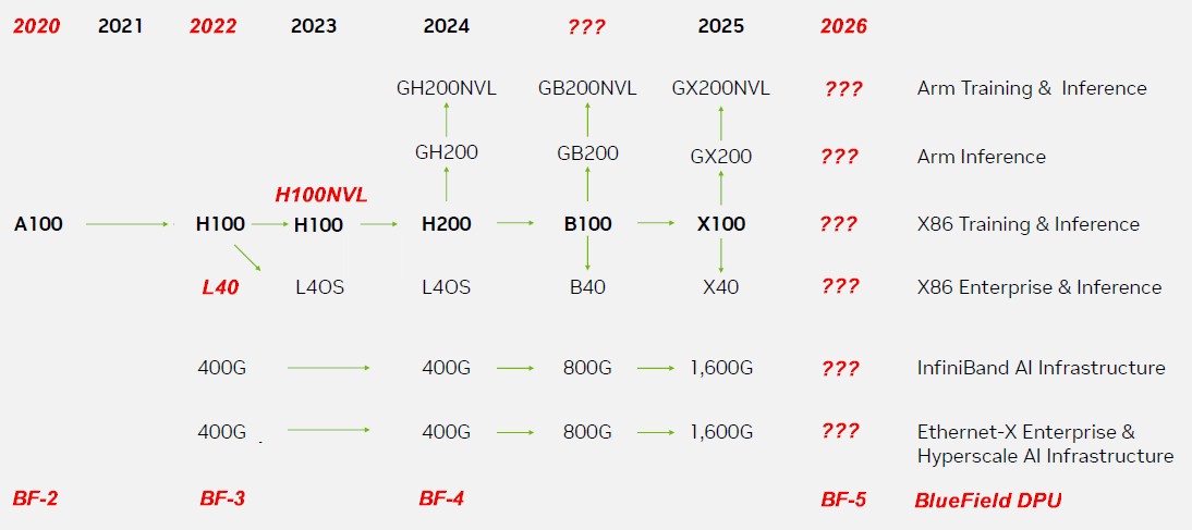
It is clear that the generative AI explosion has removed the hesitancy in the upper echelons of datacenter and supercomputing for both compute and interconnects. So an annual cadence makes sense. But it may be very hard to maintain without some slippage. In fact, this roadmap could be viewed as a way to cover for slippage in the delivery of the Blackwell architecture, and the fact that the Xavier GX100 is coming in 2025, perhaps very close to Blackwell, tells you something is up. Perhaps Nvidia will switch to fall announcement and delivery of its datacenter GPUs starting with Blackwell? The H200 GPU accelerator, whatever it is, is noteworthy in that there is no B200 or X200 following it. This H200 is a one trick pony. Well, unless Nvidia gets into another bind. . . .
Here is something to consider: The cadence of the roadmap doesn’t matter as much as the volume of the supply when the demand for a product is somewhere like 3X, or 4X, or even maybe 5X what you can deliver. If the clouds and a few AI startups get all of the Hopper GPUs and no one else can, then so what? That means there is an opportunity for anyone with anything that has a matrix math engine and an AI framework to sell whatever they got.
And so, we see just that happening, even with dead-end products like Intel’s very well regarded Gaudi line of accelerators. Yes, Gaudi 2 can hold its own against Nvidia A100s and maybe even H100s, and yes there is a Gaudi 3 around the corner that will provide 2X the performance, but so what? There is no Gaudi 4 – but there is a GPU called “Falcon Shores” with Gaudi matrix math units and Gaudi Ethernet interconnect. Under normal circumstances, no one would buy Gaudi 2. But in the generative AI gold rush, any matrix math unit you can get will have to do.
Having picked at this roadmap a bit, this is perhaps the most important thing. Nvidia has lot of cash to corner the market for HBM memory and CoWoS packaging and keep well ahead of its competitors who also need these components to build their accelerators. It has access to forthcoming components, like the very interesting CoWoS-L packaging technology from Taiwan Semiconductor Manufacturing Co, which allows for relatively normal substrate packaging of chiplets but with baby interposers set between chiplets where there is a need for lots of wires to drive high bandwidth between parts of those chiplets. (CoWoS-L is a bit like Intel’s EMIB.) It has the cash to create a two chip H200 and a four chiplet B100 if it wants to. Nvidia has demonstrated the viability of a four-GPU design, but to be fair, the MI300X shows AMD can do it with eight chiplets stacked on top of a giant was of L3 cache.
Nvidia better not be messing around because when it comes to hardware, AMD sure as hell isn’t. And those who love open source frameworks and models are looking pretty hard at the PyTorch 2.0 framework and the LLaMA 2 large language model, which have no encumbrances whatsoever thanks to the enlightened self-interest of Meta Platforms. PyTorch apparently runs pretty well on AMD iron, and will do better on MI300A and MI300X we think.
And hence, the pace of Nvidia silicon is indeed picking up to an annual upgrade cadence starting in earnest in 2024.
Remember: You can build a moat, but you can’t drink it when the well runs dry because the water is fetid, possibly from the bodies of your enemies.


Nah, nV has decent CPUs now, the DPU has srrved it’s purpose. No more need for it.
I like Elizabeth Blackwell too (as namesake), but think it may actually be David Blackwell who won the John von Neumann Theory Prize from the Operations Research Society of America instead (or both? … a multi-namesake!).
For Xavier, I’m leaning towards Charles Xavier Thomas de Colmar of the arithmometer (as Blaise Pascal is to the Pascalene).
David Blackwell sound right
Believe the years in the roadmap are Nvidia’s fiscal years, not calendar years
That has never been true before.
I meant the latest roadmap. Things line up much better using fiscal years and based on the context from Nvidia’s announcement, it might be true this time.
Understood. But I don’t see it that way. The GPUs are early in a named year in the chart, just like GTC is early in a calendar year and when the new GPUs have come out. The Nvidia fiscal year ends in January of that year, so we are in 2024 now and clearly GH200 is not here in early fiscal 2024.
David Harold Blackwell is the scientist/mathematician and NVIDIA® Jetson AGX Xavier(Already Released) is not what the X is for there as Nvidia has not decided so X is just as Place Holder!
This is just too egregious for glaring mistakes for any Professional Industry Journalist to make!
I believe I did in fact conjecture that it was a variable. I don’t see what your particular problem is. Also, I think there are more than one possible sources for Blackwell, and a reader instantly prompted me about David Blackwell and it is in the comments. I think we’re good here.
Nvidia should open it up for a vote I think. Some folks could vote for Marvell’s Professor X, but I’d go for Professor Popkiss, after the prescient inventor of the uniquely multi-environment, airbreathing, retrorocketed, VTOL, Clear-Vu, almost self-driving, vehicle: Supercar! Jetson is just a bit too cartoony … and C. Scarlet’s self-healing retrometabolism feels a bit too “out-there”! 8^b
What are you talking about the Jetson line is already in its latest iteration and that Jensen/Xavier branding is already utilized for some time now. Can the “technology” press be a little more accurate and with some regards to their due diligence. And Reporters used to have notebooks with such information and kept that with them there with information about product code names/product branding and especially Nvidia’s Naming for it’s GPU Micro-Architectures where there’s good documentation there for that.
I do not like the trends here with the Independent Tech Press becoming too Mind Share for hire oriented rather than Just the Facts Oriented. And really there the tech press outside of the paywall has slid into that abyss where accuracy is just getting in that way of the Marketing!
Why is the Tech Press not focused on TSMC’s part of the AI product shortages with that TSMC CoWoS packaging capacity shortage there and how that affects competition in an AI Accelerator Market that the French, and probably other, regulators are looking at! And Why is one business entity able to buy up most of the packaging/fabrication capacity there to the possible detriment of competition. And the US is definitely targeting Chip Packaging IP as part of the chips act funding but TSMC needs to be in front of a US Congressional Committee explaining just why that CoWoS capacity was not properly planned out in advance for the demand that the AI boom has placed on that limited capacity from only one IP supplier. Intel’s CEO sure made a good move there with regards to Intel maintaining it’s own In-House Chip/Chiplet Packaging IP and capacity but will Intel be willing to let others get at that packaging capacity as a service? And maybe the move towards some standardization for chiplet packaging IP needs to forced upon the industry in the name of Public Utility as the world economy is so dependent on Processors and how those are Packaged.
I think there has been plenty talk about the issues with CoWoS. And I am saying it is a problem with Nvidia being able to hog capacity for HBM and CoWoS. So I am not exactly sure what your problem is. This is not SemiAnalysis — this is The Next Platform, and we are one level higher up in the stack.
As far as I know, no one else knows what the X stands for. I merely said — with humor — to re-use Xavier because it was fun. Lighten up.
Think you’re reaching pretty hard here…
I know you’re tired, hell knows I would be; but I think you meant “11 years”. Not “21 years” (2012-2023).
Also: please don’t take that as criticism, I’ve read your articles for YEARS and love your insights into an industry I love so much! Thank you, Mr. Timothy Prickett Morgan!
You’re good. We are all part of one big run of Newton’s Method of Approximation on reality. Together, we get the right curves plotted.
I think a lot of credit is being ascribed to AMD GPUs — before they have shipped.
Nvidia has shown a pretty canny ability to box competitive GPUs up and marginalize them in a way they can neither earn share nor reasonable margins in PC Graphics. Now the volume opportunity is shifting to data center, a market Nvidia pretty much built single handedly and understands like few others. AMD already is in the lead? Come on TMP.
Not saying AMD won’t get some traction, they can just simply because of all the unsatisfied demand, but I’m not sure how the upstart gets elevated to incumbent-like status? An HBM device is an HBM device. AMD isn’t magically getting more from those 1024 I/O pins than anyone else can.
We all need hope, and we love to root for the underdog. But with Nvidia’s platform lead in Data Center compute — AMD basically has been able to garner low single digits of traction from the last 3 or 4 Instinct generations — I’m going to be from Missouri here with respect to MI300. Show me.
And AMD, for real, grow some balls and submit to MLPerf. Then we’ll know you have a real part. Until then it’s all just posturing.
Nvidia just got Professor X and Aquaman to hypnotize the world with their spiralling eyeballs (I think)! q^8