

If you look back at it now, especially with the advent of massively parallel computing on GPUs, maybe the techies at Tera Computing and then Cray had the right idea with their “ThreadStorm” massively threaded processors and high bandwidth interconnects.
Given that many of the neural networks that are created by AI frameworks are themselves graphs – the kinds with vertices with data and edges showing the relationships between the data, not something generated in Excel – or output what amounts to a graph, maybe, in the end, what we need is a really good graph processor. Or, maybe millions of them.
Gasp! Who speaks such heresy in a world where the Nvidia GPU and its wannabes are the universal unguent to solve – salve, surely? – our modern computing problems? Well, we do. While GPUs excel at dense matrix high precision floating point math that dominates HPC simulation and modeling, a lot of the data that underpins AI frameworks is sparse and lower precision to boot. And given this, maybe there are better ways to do this.
The US Defense Advanced Research Projects Agency, the research and development arm of the Department of Defense, explores just such cutting edge questions, and has been looking into creating a massively parallel graph processor and interconnect since establishing the Hierarchical Identify Verify Exploit (HIVE) project back in 2017. Intel was chosen to make the HIVE processor and Lincoln Laboratory at MIT and Amazon Web Services were chosen to create and host a trillion-edge graph dataset for a system based on such processors to chew on.
At Hot Chips 2023 this week, Intel was showing off the processor it created for the HIVE project, which was originally codenamed “Puma” in relation to the Programmable Integrated Unified Memory Architecture (PIUMA) that underpins it. In August 2019, Intel gave an update on the PIUMA chip at DARPA’s ERI Summit, and at the IEEE’s High Performance Extreme Computing 2020 event in September 2020, Intel researchers Balasubramanian Seshasayee, Joshua Fryman, and Ibrahim Hur gave a presentation called Hash Table Scalability on Intel PIUMA, which is behind an IEEE paywall but which gave an overview of the processor, and a paper called PIUMA: Programmable Integrated Unified Memory Architecture, which is not behind a paywall. These were vague about the architecture of the PIUMA system. But this week, Jason Howard, a principal engineer at Intel, gave an update on the PIUMA processor and system, including a photonics interconnect that Intel has created in conjunction with Ayar Labs to lash an enormous number of processors together.
In the IEEE paper, the PIUMA researchers made no bones about the fact that they were absolutely inspired by the Cray XMT line. The XMT line from a decade ago culminated with a massive shared memory thread monster that was perfect for graph analysis, which had up to 8,192 processors, each with 128 threads running at 500 MHz, plugging into an AMD Rev F socket used by the Opteron 8000 series of X86 CPUs all lashed together with a custom “SeaStar2+” torus interconnect that delivered 1.05 million threads and 512 TB of shared main memory for a graph to stretch its legs upon. As far as Linux was concerned, this looked like a single CPU.
What’s old is new again with the PIUMA project, and this time the processor is more modest but the interconnect is much better. And presumably the price/performance is as well, and for the love of all that is holy in heaven, perhaps Intel will commercialize this PIUMA system and really shake things up.
Taking Smaller Bytes Of Memory
When Intel started out designing the PIUMA chip, according to Howard, the researchers working on the HIVE project realized that graph jobs were not just massively parallel, but embarrassingly parallel, which means there were probably some ways to exploit that parallelism to drive up the performance of graph analytics. When running on standard X86 processors, graph databases had very bad cache line utilization, with only 8 bytes or less of a 72 byte cache line being used over 80 percent of the time a graph database was running. Having lots and lots of branches in the instruction flow put stress on the CPU pipelines and the memory subsystem also had a lot of pressure on it from long chains of dependent loads, which thrashed the caches on the CPUs.
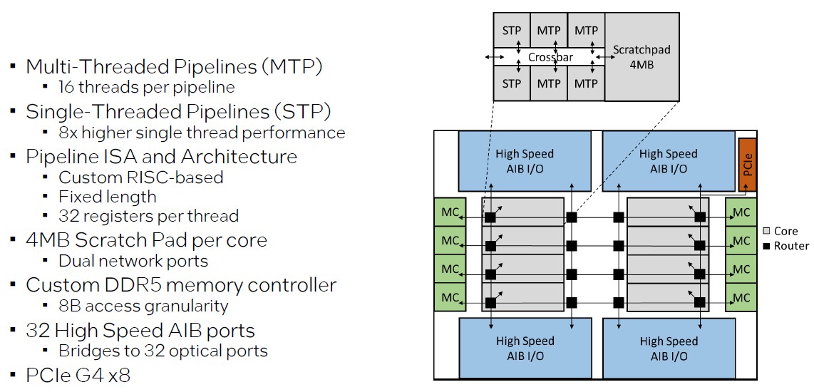
The PIUMA chip has some big-little ideas embedded with it, and has four pipelines that have 16 threads per pipeline (called MTPs) and two pipelines that have a single thread each (called STPs) that deliver 8X the performance of one of the threads within the MTPs. The cores are based on a custom RISC instruction set, which Howard did not identify and neither have his research peers at Intel or Microsoft, which has also had a hand in the PIUMA effort.
“All the pipelines use a custom ISA, it’s RISC-like, it’s a fixed length,” explained Howard in his Hot Chips presentation. “And each of the pipeline has 32 physical registers available to it. We did this so that you could easily migrate compute threads between any of the pipelines. So maybe I start out executing on one of the multithreaded pipelines and if I see that it’s taking too long, or maybe it’s the last thread available, I can migrate that quickly over to my single thread pipeline to get better performance.”
The STP and MTP units are connected by a crossbar and have a combined 192 KB of L1 instruction and L1 data cache, and they link to a shared 4 MB scratchpad SRAM memory that is simpler than an L2 cache.
Each PIUMA chip has active eight cores, and each core has its own custom DDR5 memory controller that has 8 byte access granularity instead of 72 byte granularity like normal DDR5 memory controllers do. Each socket has 32 GB of that custom DDR5-4400 memory.
Each core has a pair of routers that link the cores in a 2D mesh to each other, to the eight memory controllers, and to four high speed Advanced Interface Bus (AIB) ports. AIB is a royalty-free PHY for interconnecting chiplets that Intel announced back in 2018. There are 32 optical I/O ports, eight per AIB, that come off the die complements of Ayar Labs, which deliver 32 GB/sec of bandwidth in each direction.
Here is a drilldown on the on-chip routers that implement the 2D mesh on the PIUMA package:
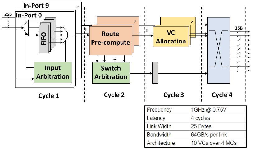
This is a ten port, cut-through router The 2D mesh runs at 1 GHz and it takes four cycles to traverse the router. It has ten virtual channels and four different message classes, which Howard says avoids any deadlocks on the mesh and which yield 64 GB/sec for every link within the router.
The router and core packaging on the PIUMA chip is a bit more complex than you might expect. Take a look:
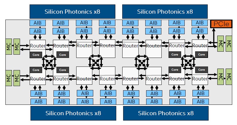
It is more like there are sixteen core/router units on the die, and only eight of them have the cores activated because the on-die mesh needs twice as many routers to feed into the AIBs, which in turn feed into the Ayar Labs silicon photonics. The silicon photonics links are only used as a physical layer, and they are used specifically to extend the on-die network between multiple sockets.
And when we say multiple, we mean a freaking huge number. Like this:
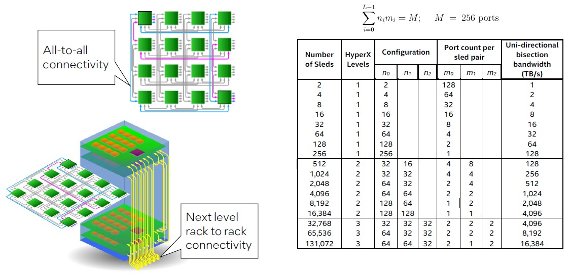
A sled of sixteen these PIUMA chips using the silicon photonics links can be linked together in a 4×4 grid in an all-to-all configuration. Each PIUMA chip burns around 75 watts at nominal voltage and workloads, which means a it burns around 1,200 watts. More than a Xeon SP socket, but not more than three of them.
Building The Perfect Graph Processing Beast
The PIUMA chip has 1 TB/sec of optical interconnect coming out of it, and aside from the on-sled links, some of them can be used to connect up to 131,072 sleds together to make a massive shared memory graph processing supercomputer. The routers are the network, and everything is connected by a HyperX topology outside of the directly connected-all-to-all topology within a rack, which has sixteen sleds.
Let’s walk through this. A single sled with sixteen sockets has 128 cores with 8,448 threads and 512 GB of memory. The first level of the HyperX network has 256 sleds, 32,768 cores, 270,336 threads, and 128 TB of memory. Step up to level two of the HyperX network, and you can build out a PIUMA cluster with 16,384 sleds, 2.1 million cores, 17.3 million threads, and 8 PB of shared memory. And finally, up at level three of the HyperX network, you can expand out to 131,072 sleds, 16.8 million cores, 138.4 million threads, and 64 PB of shared memory.
Admit it. You want to see what one of these beasts could do. The US National Security Agency and the Department of Defense in the United States and their peers around the world, who have funded a lot of the AI research in the past fifteen years, no doubt are interested, too.
As you chew on that scale for a minute, let’s go over a few more things. First, the latency of that optical network:
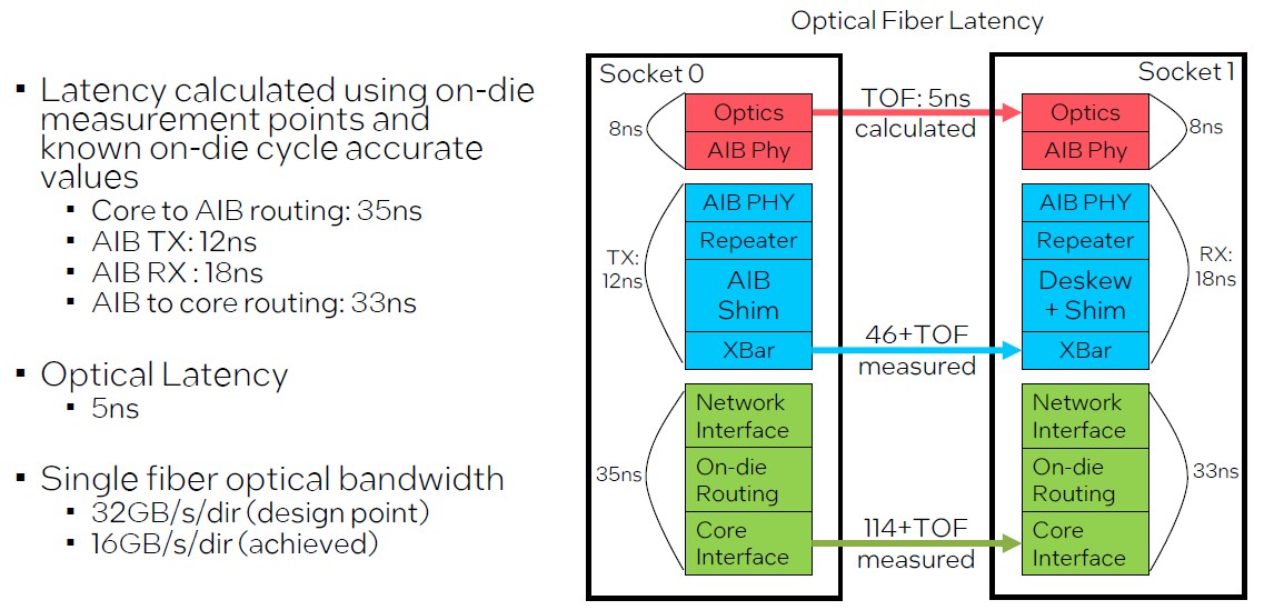
The PIUMA nodes are linked together with single-mode optical fiber, and it is interesting that the achieved bandwidth of the PIUMA network design, at 16 GB/sec per direction, was only have the of the theoretical design point. But even still, this is a huge bandwidth beast, with a theoretical 16 PB/sec of uni-directional bisection bandwidth across the full HyperX network.
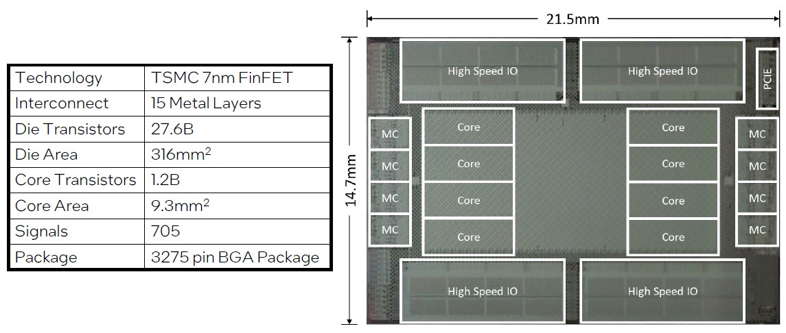
The PIUMA chip is implemented in 7 nanometer FinFET processes from Taiwan Semiconductor Manufacturing Co, and it has 27.6 billion transistors on it with 1.2 billion of them being dedicated to the relatively small cores. The AIB circuits take up a lot of the transistor count, apparently.
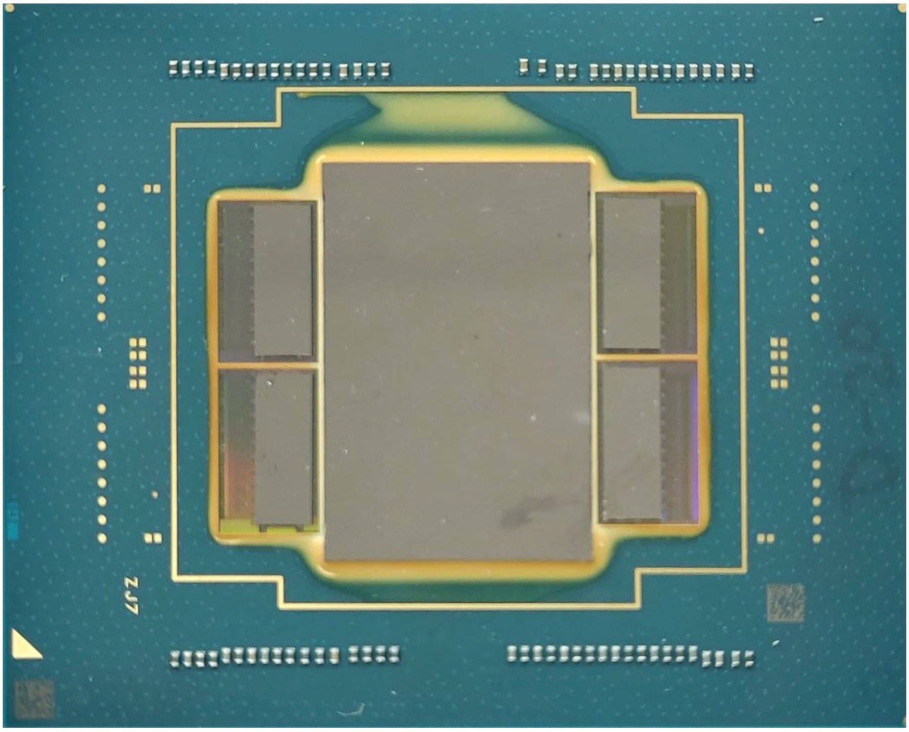
Here is what the PIUMA chip package looks like:
And here is what the package and test boards look like:
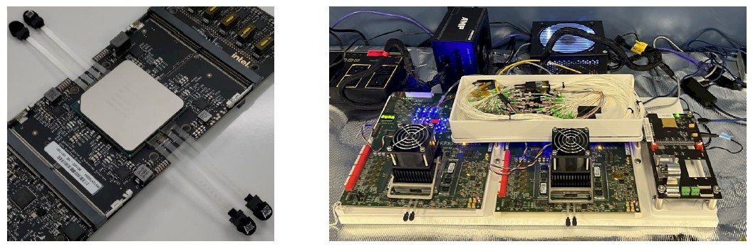
So far, Intel has built two boards with a single PIUMA chip each and interlinked them to runs its tests and to prove to DARPA that it works.
The question now is, what will such a machine cost at scale? Well, at $750 per node, which ain’t much at all, it is $3.1 million for a system extended to HyperX level one with 4,096 PIUMA chips, close to $200 million for one with 262,144 chips at HyperX level two, and $1.57 billion for one with 2.1 million chips stretched to HyperX level three.
As the generative AI explosion shows, there are several dozen companies and then another several dozen government agencies in the world that won’t even blink at $1 billion for a system anymore. The number didn’t even raise my pulse when I wrote it and then read it.
That’s just the time we live in now.


Hello Mr. Morgan,
you do not need to publish this…just want to tell you a typo I found while overflying some articles before reading, also yours here:
” The XMT line from a decade ago culminated with a massive shared memory thread monster that was perfect for graph analysis, which had up to 8,192 processors, each with 128 threads running at 500 GHz”
->I think my technically interested part would like to see such a thing as much as you, for sure, but I think, as I overflew the ElReg article, it should be MHz
Yup, I would love to see that too. HA! No, it was 500 MHz for the XMT.
500 GHZ!!!
I’ll take a dozen, please.
Thank you TPM, I Really enjoyed this article.
I was confused with the use of the phrase ‘core complex’; would it be possible to elaborate on this.
That’s because I didn’t use the term correctly. All fixed.
Interesting outside-the-box innovative stuff (retro-futuristic?), especially as graphs and arborescence are key to so many computations, as noted here last month by Tenstorrent’s Jim Keller. I like the improvements that these newfangled thingamabobs bring to prior cuckoos (ahem: https://www.theregister.com/2011/02/20/cscs_cray_xmt_2/), especially the Co-Packaged Optics (CPO), 8-byte-granular DDR5, and the combo of single- and multi-thread pipelines.
Heavy multi-threading pretty much did SUN in back in the Niagara days I think, because of CMT’s poor performance on common single-threaded workloads (though CMT is probably great for graph-oriented Oracle database analysis and search applications). Combining single- and multi-threaded pipelines in one chip, as in this computational feline, looks like a more balanced way to prowl through both tree and trail.
CPO is one of those oft-promised techs that we seem to be just “way behind” on (permanently in the next 2-5 years) and I’m glad Intel/Ayar jumped right in to figure out the right materials, techniques, and tools for this hybrid packaging, as needed to foster composable disaggregation of heterogeneous cephalopods (computational units). Google’s TPUs already demonstrated several tangible benefits of this kind of flexible optical networking (if I read that previous article well).
I’m not sure how they approached 8-byte granularity on DDR5, but if it means eight 8-bit wide channels read independently via burst-8 (octal data rate), then that could also be a winner (not sure how else this could be done really)!
IMHO, a key to future systems (next platforms) will be in how these retro-futuristic innovations can be woven into and merged with current single-threaded, large-cache-line, copper archs, so that both kinds of workloads are efficiently processed.
Yep, I can see how graphs become more important when dealing with FEMs that produce irregular sparse matrices (unlike regular sparsity of FDM, tackled by ADI) and in pruned/culled AI models — block-based memory accesses then naturally give way to retro-futuristic kung-fu!
P.S. A most happy of Labor Days to folks in North America (best holiday of the year)!
For my money, I’d say 32-byte memory access granularity and cache-line size may the sweet-spot for mixed graph-based and non-graph workloads, somewhere between this PIUMA’s 8-byte and the more common 64-byte. At 64-bit, the LISP-standard cons-cell (car+cdr pointers for lists and trees) is 16-byte, and a N-E-S-W pointer-cell for quadtrees is a 32-byte item, both a better fit to 32B than 64B cache-lines (the main drawback being “moderately” more die-area for cache tags). 32-Byte also matches the 256-bit vector length that some seem to be standardizing on (eg. AVX10, Neoverse V1 TRM), and is already the line size of cache “sectors” in some high-performing xPUs (POWER9, Fermi, Kepler, …).
The DDR5+ DIMM could then be an MCR job with four independent 32-bit channels (same num of 32b chans as an HBM3 die), 8x pumped, so each channel fills a 32B cache line per burst. This should give a 2x to 8x perf boost on graphs, without slowing down linear jobs. As a bonus, 8 of these DIMMs would essentially mimick an 8-die HBM3 single-stack (32x 32b chans). Extra graph-grit might then come from many-threading, if really desired (and double-checked).
The CPU-design pros could surely do worse than simulate such a system to verify its most awesome in the world of mixed-load oomphs, prior to fabbing it in the commensurate volumes it truly deserves!
Hi,
I believe the numbers for the RAM are not correct:
> Let’s walk through this.
> A single sled with sixteen sockets has 128 cores with 8,448 threads and 512 GB of memory.
> The first level of the HyperX network has 256 sleds, 32,768 cores, 270,336 threads, and 1 TB of memory.
> Step up to level two of the HyperX network, and you can build out a PIUMA cluster with 16,384 sleds, 2.1 million cores, 17.3 million threads, and 64 TB of shared memory.
> And finally, up at level three of the HyperX network, you can expand out to 131,072 sleds, 16.8 million cores, 138.4 million threads, and 512 PB of shared memory.
1 sled: 512GB (seems correct from what I can read from the beginning of the article)
256 sleds the 1TB should be 128TB
16,384 sleds the 64TB should be 8PB
131,072 sleds the 512 PB should be 64PB
Or maybe there is something I’ve misunderstood?
Nope. You’re right. I pointed to cores in my sheets instead of chips for the higher two numbers.