
What is the hardest job at Intel, excepting whoever is in charge of the development of chip etching processes and the foundries that implement it? We think it is running its disparate networking business. The competition is tough, and getting tougher with both incumbent and upstart players taking on Intel in network interface cards, switching, silicon photonics, and other areas.
Hong Hou is the new general manager of Intel’s Connectivity Group, one of the sub-fiefdoms in the Data Center Group, which all told drove $27.71 billion in revenues in the trailing twelve months, or more than a third of revenues but more than half of the company’s overall profits.
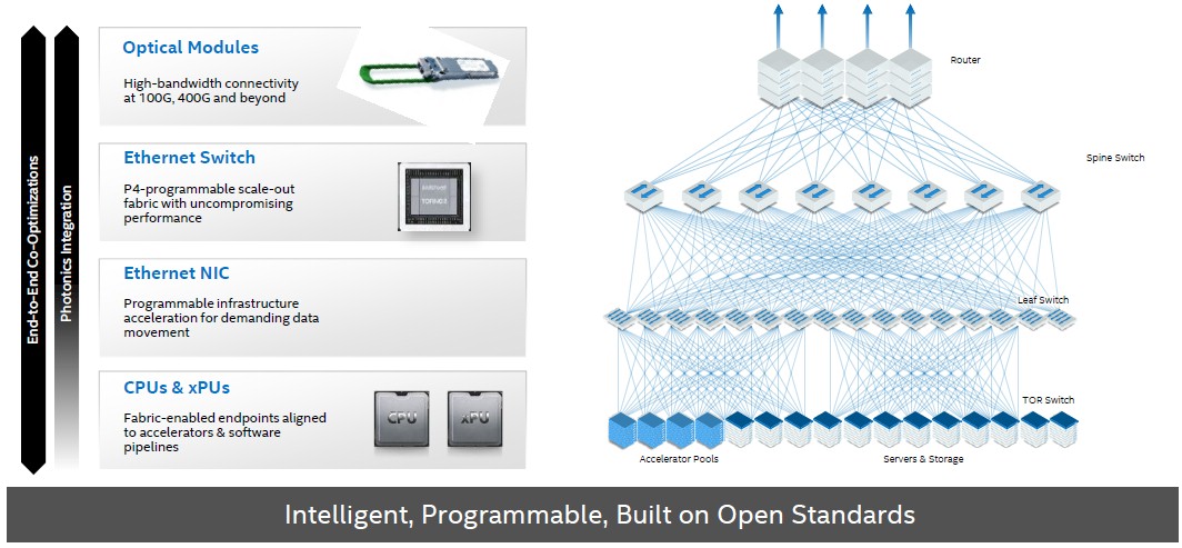
We don’t know how much of this Data Center Group business is networking in its various forms, but we suspect it reflects the industry at large to a certain extent and then skewed to the right a bit towards compute and away from networking and storage. It is hard to guess how much the networking business in the aggregate makes – we don’t have enough data and it depends on how you cut it. It has a network interface card business that rivals the Mellanox division of Nvidia, and a switch business that is probably on par with Mellanox if you include Barefoot and Omni-Path together. Silicon photonics is not yet driving a lot of revenues, but transceivers for network cables probably does.
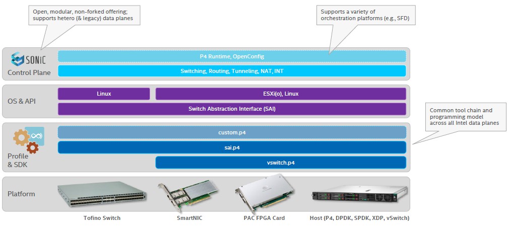
There is no easy way to quantify how much software-defined networking software is running on Xeon iron, either, which is technically should be counted as Connectivity Group revenues, or how much networking is supported by its Data Plane Development Kit and other systems software, or how much of the sales of its (formerly Altera) FPGAs are being sold for networking use cases. But Intel is trying to build a networking software stack, based on various SDKs, operating systems and abstraction layers, and control planes that run across its various networking hardware. Take a gander:
Suffice it to say, despite the challenges, Intel is a player in interconnects even if it is not the dominate one. Markets are generally not well served by such dominance, anyway, in terms of the pace of innovation and the cost of that innovation. So it is not a desired state of affairs. But, it absolutely is desirable to have Intel be in the networking business and bring what it knows about the datacenter to bear.
Hou takes on a Connectivity Group that is undergoing a lot of change. Intel built an arsenal of HPC-style networking in 2011 and 2012, including the QLogic InfiniBand business and the Cray “Gemini” XT and “Aries” XC interconnects, which it sought to merge into a super-interconnect called Omni-Path but which it has just spun-out to Cornelis Networks, founded some former Intel and QLogic employees. With many of the exascale-class supercomputers using Hewlett Packard Enterprise’s Cray 200 Gb/sec Slingshot HPC variant of Ethernet and most of the remaining companies using 200 Gb/sec HDR Quantum InfiniBand, it is no surprise that Intel would let Omni-Path go into the history books; what was more surprising is that Cornelis Networks wants to take the ideas of InfiniBand and Aries interconnects and carry it forward in its own direction.
The handwriting was on the wall with Omni-Path inside of Intel in June 2019 when the company bought Barefoot Networks for its programmable Ethernet switch ASICs and to get more control of the P4 programming language for switches. Intel is more interested in programmable Ethernet switching and SmartNICs (increasingly called DPUs) for hyperscalers and cloud builders, which will be eventually mimicked by other service providers and large enterprises as the technology waterfalls down from on high.
That is the idea, anyway.
Here is the reality: Companies will splurge on compute, by which we generally mean CPUs but increasingly GPUs and occasionally FPGAs, rather than memory or networking because they understand it better. Here is another fact that cannot be bargained with: The amount of data that is being shuttled around by networks in the datacenter is growing at 25 percent per year. But budgets cannot grow at that rate, and moreover, because of the prejudicial investment in raw CPU compute – as opposed to building balanced systems that more fully utilize whatever compute is available – networking is not usually more than 10 percent of the cost of a distributed system, and when it does get up to around 15 percent, there is a lot of weeping and gnashing of teeth.
It is against all of these pressures that Intel must innovate and help improve networking. And integration is going to be one of those keys, according to Hou.
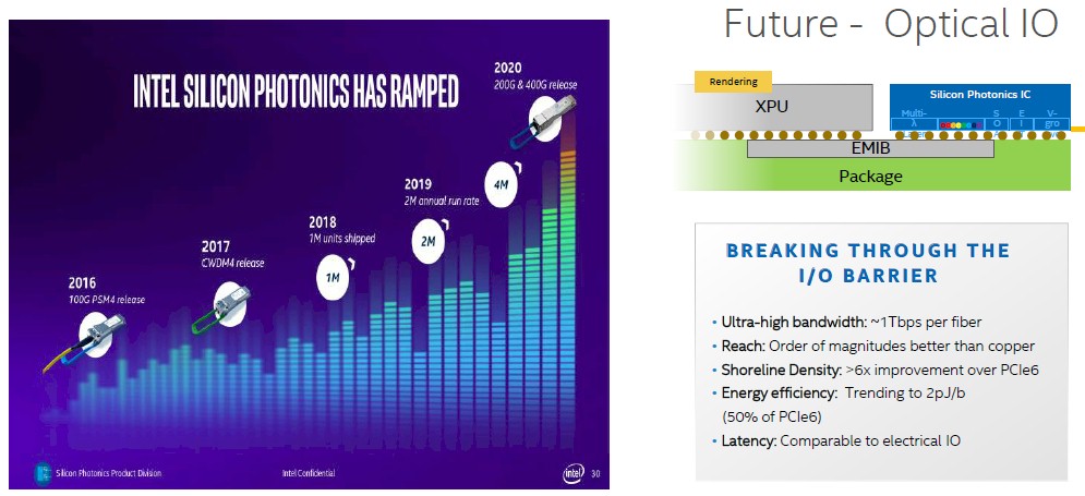
 “For Intel, we want to provide intelligence and programmability in a flexible network that can handle the complexity of the emerging workloads,” Hou tells The Next Platform. “Our vision is to optimize all of these technology assets to provide enabling solutions for our customers –we are not just a supplier of a bag of parts. So let’s fast forward by five years. Ethernet is going to evolve from just end point connectivity abd will enter the CPU from a SmartNIC, or whatever we might end up calling it, to offload some critical workload and to accelerate some of the workloads and to provide that performance enhancement for the network. This SmartNIC will integrate with CPUs, GPUs, FPGAs for compute and there may also be memory devices. We see that clear trend, and we are putting concerted effort in our development. Later on, we’ll talk about our new product release based on FPGA. Back in March, we announced the co-packaging of the optics with the switch, and that has been received very well. The next step is going to be using the optical I/O technology to provide more bandwidth density. The electrical die-to-die interconnect may run out of steam and may not be able to provide the connectivity for the data volume needed. So we need to have the optical I/O to support the traffic.”
To a certain extent, the hardware is the easy part. While the interconnect industry has picked up the pace in recent years – there was some signaling roadblocks a decade ago that caused a massive slowdown in innovation – and we can now expect a cadence of switch ASICs and matching network interface ASICs every 18 to 24 months. But, says Hong, network operators inside datacenters want the pace of innovation to be faster, and they want to innovate in software as well as in hardware, as they have been able to do in the compute part of the datacenter stack for decades. So programmability – and therefore P4 – is just as important as how many transistors you can cram down onto a switch or network interface ASIC and what you do with them.
When it comes to the “Tofino” family of Barefoot switch ASICs, Hou says that customers are telling Intel to stick to a two-year cadence on chip rollouts. The 6.4 Tb/sec Tofino 1 chip started sampling when Barefoot dropped out of stealth back in June 2016, as 2018 was coming to a close, the 12.8 Tb/sec Tofino 2 chips were unveiled, employing a chiplet design breaking the SerDes from the packet processing engines, and using 25 Gb/sec native signaling plus PAM-4 encoding to get an effective 50 Gb/sec per lane. The resulting switches could drive 32 ports at 400 Gb/sec or downshift the speeds and uplift the port counts proportionately.
There might be a bit of a delay in that two-year cadence because of the Intel acquisition and the as-yet impending decision to do optics co-packaging with the Tofino ASIC at either the 25.6 Tb/sec Tofino 3 generation (that’s 32 ports at 800 Gb/sec) or the 51.2 Tb/sec Tofino 4 generation (that’s 32 ports at a stunning 1.6 Tb/sec). To get to these speeds is going to require 112 Gb/sec native raw signaling plus either denser PAM encoding or more lanes for port – we will see what happens. But Hou is pretty confident that Intel can get a 102.4 Tb/sec Tofino 5 into the field at some point in the future. If you do the two-year cadence, Tofino 2 is sampling now and will be in products in 2021, Tofino 3 will sample in 2022 with products in 2023, Tofino 4 will sample in 2024 with products in 2025, and Tofino 5 will sample in 2026 with products in 2027. At that point, datacenter networking will hit the same absolute wall that datacenter compute will. Get your thinking caps out, people.
In the meantime, in an aside in a press release and something that Hou did not bring up when we chatted, “will open source the Tofino architecture to ensure programmable packet processors are as open as CPUs.” First of all, open source what? The actual chip design or whatever passes for an instruction set in a switch ASIC? And second, “as open as a CPU?” None of Intel’s processors are open source, nor are AMD’s, and nothing based on Arm is but the technology is licensable and adaptable. IBM has open source the Power ISA and two Power cores, the A2I and the A2O, based on its PowerPC-A2 architecture and used in network processors and the BlueGene/Q supercomputer. Sun Microsystems open sourced the “Niagara” T1 multithreaded CPU way back when. We will try to figure out what Intel is talking about.
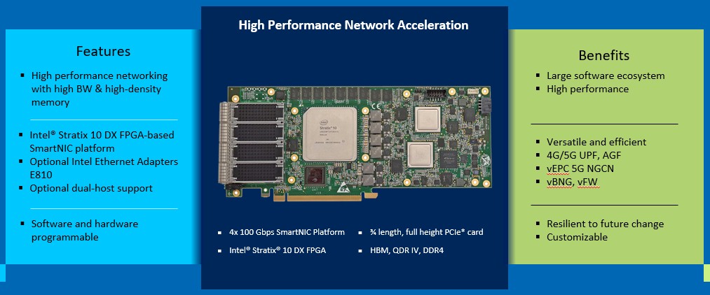
All of this brings us, in a roundabout way, to SmartNICs or DPUs, whatever you want to call them. Let’s get philosophical for a moment. DPU is only a good term if you are literally etching a new type of chip that is really doing some data handling and processing in a different way from a switch or router ASIC, or a CPU or a GPU for that matter. (An FPGA can pretend to be anything, so you can’t really exclude or include this device.) Fungible seems to be creating a real DPU, which we discussed here at length with the company’s founder, and Pensando seems to be doing the same. Intel and Nvidia and others are creating SmartNICs that combine various elements together. For Nvidia, it is combining an Arm CPU with a ConnectX network interface chip and an Ampere GPU. And for Intel, with the latest SmartNICs that Hou gave us a preview of, combine CPUs and FPGAs and maybe, in one case unless it is a typo, a Tofino switch ASIC as well as the Intel 800 Series network interface chips into a composite compute complex one can call a DPU in the broadest sense. This is what we think the industry will do, because DPU sounds smarter and cooler and more valuable than SmartNIC.
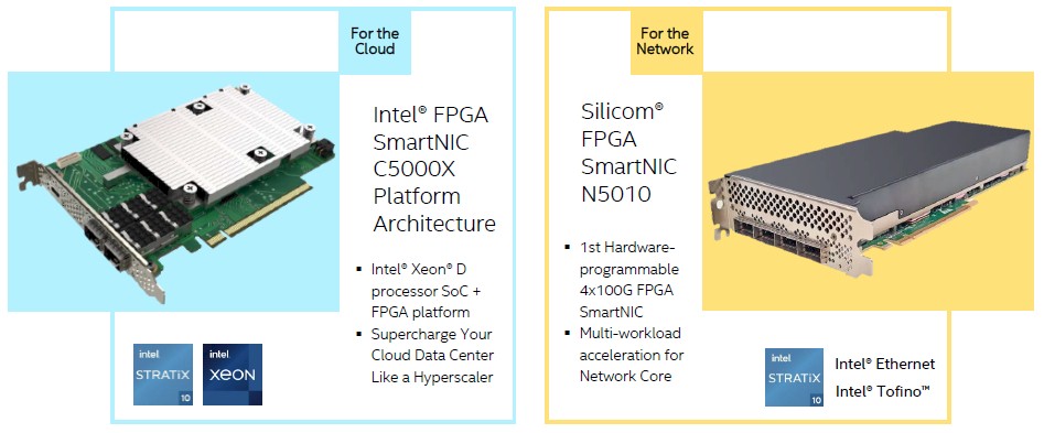
These new FPGAs are targeted generally at cloud and communication service providers, which we here at The Next Platform break into three buckets, the hyperscalers, the cloud builders, and the rest of the telco and service providers who are not quite so big but who are also not traditional enterprises like manufacturing, distribution, and such.
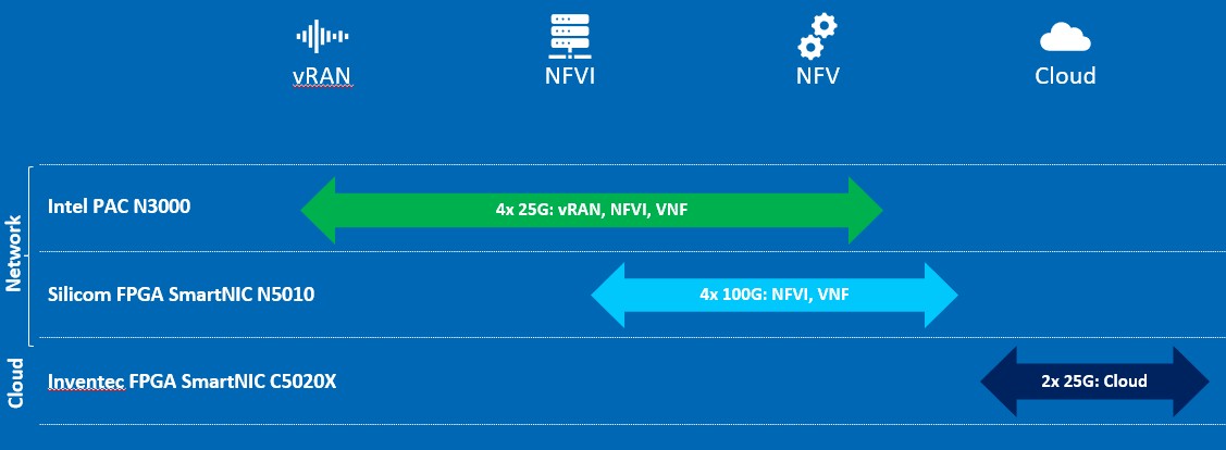
What is interesting here is that the new Intel SmartNICs are not actually made by Intel, but by Inventec and Silicom, the former being an increasingly important ODM for hyperscalers and cloud builders and the latter being a network interface supplier for the past two decades. These devices sit on a spectrum along with the pure FPGA acceleration card, called the Programmable Acceleration Card, which we talked about when it first debuted with the Arria 10 FPGA in October 2017 and when it was updated in September 2018 with the Stratix 10 FPGA. Here is the FPGA acceleration continuum as Intel sees it:
The SmartNIC C5020X for the cloud looks and smells like something that was made for Facebook – any time you see Xeon D, think Facebook since this chip was basically designed and kept alive for the social network, to such an extent that it should just be called the Xeon F really. That said, Microsoft also gave a blessing of sorts to this particularly SmartNIC, so maybe they are both going to use it.
Here are the features of the SmartNIC C5020X from Inventec:

And here is the block diagram for a deeper look:
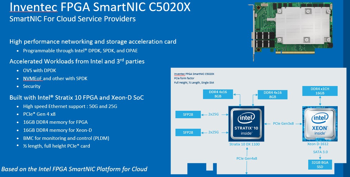
The Stratix 10 DX 1100 is the low end FPGA in this family of devices, with over 1.3 million logical elements and on the order of 10.4 TMACS (trillions of multiply accumulates second) on fixed point work and 4.1 teraflops on 64-bit floating point math. That’s less than half of the much heftier DX 2800 FPGA. The Xeon D-1612 has four cores running at a base of 1.5 GHz and a turbo speed of 2.5 GHz. Again, this is nowhere near the beefiest Xeon D chip that Intel has. What is interesting is that the Stratix 10 has two blocks of 8 GB of DRAM memory to feed it and has two 50 Gb/sec Ethernet ports, and that the FPGA and servers link to each other over 8 lanes of PCI-Express 3.0 – mainly because the Xeon D doesn’t support PCI-Express 4.0. That Xeon D has only one memory channel, and Inventec is putting 16 GB on it. There is a 32 GB SSD flash chunk welded to the board hanging off the Xeon D. And finally, the whole complex links out to the server using a 8 lanes of PCI-Express 4.0, which no current Intel processors support but which Ice Lake will when it ships shortly and is launched generally early next year. This card could plug into machines using IBM’s “Nimbus” Power9 or AMD’s “Rome Epyc 7002 processors today, ironically.
It has been suggested that the Silicom SmartNIC N5010 has a Tofino switch ASIC on it – it shows that on the overview chart at the top – but it certainly is not in the schematics we have seen. But it would be very interesting indeed to see people ditching Open vSwitch soft switches for actual small implementations of real ASICs in the SmartNICs or DPUs of the future to get away from the slow speed of the software. As long as the baby switch is programmable – meaning that new protocols can be laid onto the hardware – this is a good split between hardware and software and is still leaning more to the software than the FPGA does.
Anyway, here are the features of the Silicom N5010 SmartNIC:
And here is the block diagram for the device:
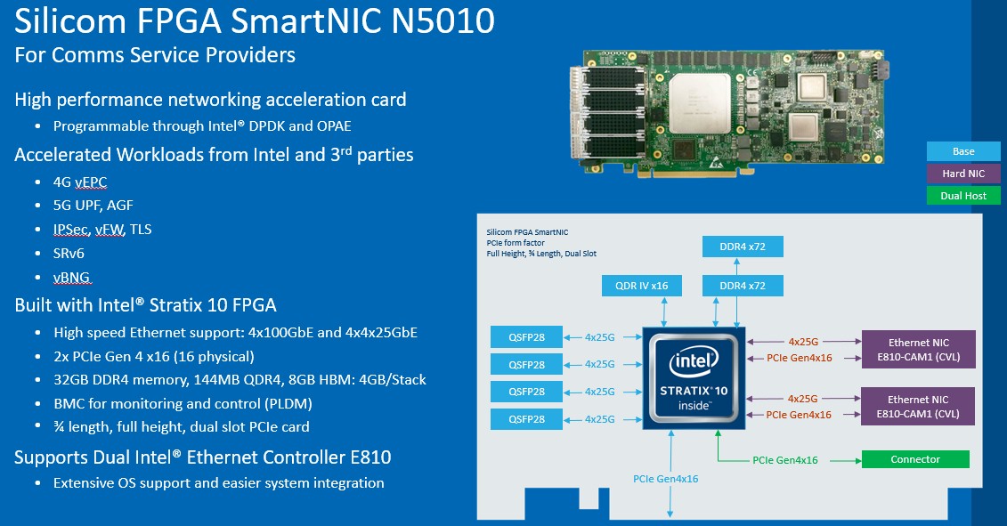
The block diagram says the two Ethernet E810 NIC ports, driven by Intel’s ASIC and running at 100 Gb/sec each, are optional and hang off the PCI-Express 4.0 lanes on the Stratix 10 FPGA. The FPGA also drives four of its own 100 Gb/sec ports, and obviously all of those ports would be a pretty heavy I/O load. This card connects back to the host system using a double-wide but only a single slot PCI-Express 4.0 slot with 16 lanes. There is another PCI-Express 4.0 x16 connector, and maybe a switch ASIC connects in here, but that seems unlikely. The FPGA has an x16 port going out to 144 MB of QDR SRAM memory, 32 GB of DDR4 memory, and 8 GB of HBM2 stacked memory. That is a lot of memory, not including the memory inherent in the FPGA blocks.
There is no word on pricing or general availability of these two SmartNICs.
One last thought: We are a zillion miles away from the onload model of networking that Intel was espousing a decade ago, which would have put more and more of this work on CPUs. The world did not agree, and Intel reacted. So offload all around!


AI At The Edge Is Different From AI In The Datacenter
Today’s pace of business requires companies to find faster ways to serve customers, gather actionable insights, increase operational efficiency, and reduce costs. Edge-to-cloud solutions running AI workloads at the edge help address this demand. Placing compute power at the network edge, close to the data creation point, makes a vital …

If You Want To Maximize Enterprise AI, Don’t Just Focus On GPUs
Paid Post There’s no doubt that the repurposing of GPU silicon has accelerated the development of artificial intelligence technology over the last decade. But focusing exclusively on GPUs when building out your own AI infrastructure can leave you with a misleading picture of what your ecosystem should really look like. GPUs are …
Intel Pushes Out Hybrid CPU-GPU Compute Beyond 2025
One of the reasons why Intel can even think about entering the GPU compute space is that the IT market, and indeed just about any market we can think of, likes to have at least three competitors. With capital intensive businesses, there is an inevitable consolidation, and sometimes only two …
Be the first to comment