

Intel has spent more than three decades evolving from the dominant provider of CPUs for personal computers to the dominant supplier of processors for servers in the datacenter. While Intel has argued that Moore’s Law is not dead – that the pace of innovation with transistors and therefore semiconductors has not slowed – even the world’s largest CPU maker has to concede that the nature of Moore’s Law advances has changed – the leaps are getting harder between process nodes for sure. This is one of the main reasons why CPUs are not expected to utterly dominate the datacenters of the future.
This is, after all, why Intel has been buying up makers of alternative compute engines in the past five years – Altera and eASIC for field programmable gate arrays and Nervana Systems and Habana Labs for neural network processors – as well as dropping the “Knights” family of parallel processors inspired by its early “Larrabee” research on X86-based graphics processors in favor of starting from scratch to create its Xe family of integrated and discrete GPUs. To be sure, Intel will continue to add features for HPC and AI to its mainline Xeon SP processors, but the company knows the future is going to be heterogeneous and is building a hardware stack and the OneAPI development tools that will allow programmers to code in C++ once and deploy to any compute engine in Intel’s arsenal.
There will be a hierarchy of heterogeneity in future systems, as Jose Alvarez, senior director in the CTO Office for the Programmable Solutions Group at Intel, sees it, and this is all a result of the shift to data-centric applications and the architectures that support them. This will be one of the themes in the keynote that Alvarez will be giving at The Next FPGA Platform event we are hosting at the Glass House in San Jose on January 22. (You can register for the event at this link, and we hope to see you there.)
“One architecture doesn’t fit everything, and there are a lot of different workloads,” Alvarez tells The Next Platform. “There are scalar, vector, matrix, and spatial architectures and those are very uniquely positioned to solve multiple problems. For scalar, you may use a CPU. For vector processing, you may use a GPU. For matrix, you may use a dedicated ASIC as we do for machine learning and artificial intelligence. And for spatial, you might use an FPGA.”
That heterogeneity that Alvarez speaks of is not just across systems, with machines using different components and yet, in the future, united by OneAPI in the case of Intel’s compute engines, but within them where a system will have two or more compute components and, in some cases, says Alvarez, extends down into the devices themselves, which will be a mix of capabilities within a package.
“Monolithic semiconductors have their limitations,” Alvarez says. “They’re big, and there is a point at which they are so big that they are very difficult to manufacture. And therefore using smaller components, which are faster to develop and have better yields, is a better approach to integrate system components. And so Intel created the Embedded Multi-die Interconnect Bridge, or EMIB, and also the Advanced Interface Bus, or AIB, which is our royalty free PHY to connect chiplets at the package level. Our Foveros 3D stacking technology is also important for reusuability, as is EMIB and AIB, because the chiplet approach brings agility, a very fast way to migrate technology between devices. And we are making AIB an open standard because we want to encourage an ecosystem to develop, and the reason is that we know that we cannot do everything. This is all about creating an ecosystem of chiplets.”
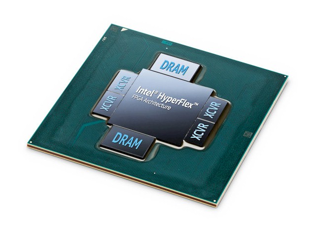
The Stratix 10 family of FPGAs is pioneering some of these technologies in that it is using AIB links to connect an FPGA die with four transceiver tiles and two HBM2 stacked memory tiles all together on the same package, like this:
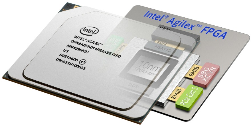
The more recent Agilex FPGAs, which launched in April 2019, use EMIB to glue the FPGA to elements of the package, including HBM2 memory, PCI-Express controllers, 112 Gb/sec transceivers, and coherent interconnects coming out of the package, like this:
There are even finer grained distinctions here. Intel has the new Agilex lineup as well as the existing Arria 10 and Stratix 10 devices for those who want to go with the pure FPGA approach, which is generally when standards and frameworks are changing fast and you need a more flexible and adaptable device to keep pace with the changes. Once things settle down, then it is time to think about a more traditional hard-etched custom ASIC to run particular algorithms. But there is still a place between an FPGA and an ASIC, called an eASIC or structured ASIC, where Intel can create something in-between these two on the spectrum of malleability. These structured ASIC devices are commonly being deployed in various networking and Internet of Things applications, and the good news is that once an FPGA is created, it can be converted into a structured ASIC using the eASIC approach. Moreover, in the long run, Intel plans to use EMIB to create compute engines that mix and match FPGA and structured ASIC components all in the same package.
All of this heterogeneity in the silicon and in the programming tools allows for FPGAs to be more easily integrated into systems and therefore the datacenter and we will finally get to see where they naturally belong in the application stack. But datacenters need more than a heterogeneity of devices and programming tools to push code to them so they can chew on data. In many cases, they need help. And that is where overlays are going to play a big part, says Alvarez.
Overlays are a kind of abstraction layer that runs on top of the FPGA and provides amounts to an instruction set for running very specific algorithms. In a sense, it is akin to a Java Virtual Machine, which has interpreted Java code that can be compiled down to bytecodes through the JVM that allow it to be executed on very different CPUs that are supporting those JVMs. FPGA overlays similarly break the functional architecture from the precise implementation of the FPGA, so the overlay is not only important because it creates something that can be deployed easily by many users, but also has the potential to create a modicum of portability across FPGA devices.
The main thing is that an overlay creates a domain specific architecture with its own domain specific language, which is how programmers and system architects are tuning applications – or probably better still, portions of applications – for specific kinds of devices.
“Domain specific architectures lead to domain specific languages, and FPGAs are uniquely positioned to implement domain specific architectures because you can do this through overlays,” explains Alvarez. “Overlays are essentially little processing engines that you can implement in an FPGA very efficiently. So, for instance, maybe you have an application where you have some GPU commands that are very important to you and you create a domain specific language to fit exactly the applications that you need. Microsoft does exactly this with its BrainWave soft DPUs. But overlays have an extra advantage. As you know, FPGAs are notoriously difficult to program, and even if you use high level synthesis, you still need to synthesize, place, and route logic, which can take hours. With a domain specific architecture and an overlay, you basically transform the problem from synthesis, place, and route to just a compilation that takes seconds or milliseconds in some cases. So you completely change the way that you develop and the FPGA is easier to program now because you are attacking this domain specific problem directly.”
This is why we think, in the long run, there will certainly be big banks of FPGAs running all kinds of things in the datacenter. It may not be that every server has an FPGA, but maybe what can be said is that every CPU that is running host applications in some manner will have access to an FPGA. And probably links to GPUs and a collection of other specialized ASICs, too. The datacenter is the new motherboard.


Same old same old diabatic transistor.
Time for new adiabatic switches.
“e” as in Energy eV 1.602176634×10⁻¹⁹ J
At 20 °C (room temperature, or 293.15 K), the Landauer limit , kTln2, represents an energy of approximately 0.0175 eV, or 2.805 zJ
Energy Recovery and Recycling in Computation: Reversible Adiabatic Logic
Physical Foundations of Landauer’s Principle by Michael P. Frank
“… the physical foundations of Landauer’s Principle, which relates the loss of information from a computational process to an increase in thermodynamic entropy. Despite the long history of the Principle, its fundamental rationale and proper interpretation remain frequently misunderstood. …”
kTn2.com
Bend the CO2 curve down one bit at a time. Now!