

The hyperscalers, cloud builders, HPC centers, and OEM server manufacturers of the world who build servers for everyone else all want, more than anything else, competition between component suppliers and a regular, predictable, almost boring cadence of new component introductions. This way, everyone can consume on a regular schedule and those ODMs and OEMs who actually manufacture the twelve million servers (and growing) consumed each year can predict demand and manage their supply chains.
As many wise people have said, however, IT organizations buy roadmaps, they don’t buy point products because they have to manage risk and get as much of it out of their products and organizations as they possibly can.
AMD left the server business for all intents and purposes in 2010 after Intel finally got a good 64-bit server chip design out the door – with the “Nehalem” Xeon E5500 architecture that came out in early 2009 largely copied from AMD’s wildly successful Opteron family of chips. AMD’s early Opterons were innovative, sporting 64-bits, multiple cores, HyperTransport interconnect, and multiple cores on a die, and essentially made Intel look like a buffoon for pushing only 32-bit Xeons and trying to get the enterprise to adopt 64-bit Itanium chips. But by 2010, AMD had been delayed on delivering several generations of Opterons and had made an architectural fork that did not pan out. When Intel pulled back on Itanium and designed many generations of competitive 64-bit Xeon server chips, AMD was basically pushed out of the datacenter. But by 2015, Intel had been slowing the pace of innovation and driving up prices, and the market was clamoring for more competition, and AMD reorganized itself and got to work creating what has become its Epyc comeback – this time once again coinciding with Intel leaving its own flanks exposed for attack because of delays in its 10 nanometer and 7 nanometer chip making processes.
Intel, under the guiding hand of chief executive officer Pat Gelsinger, is getting its chip manufacturing house in order and also getting back to a predictable and more rapid cadence of performance and feature enhancements, and that means AMD has to do the same thing. And as part of its Data Center Premier event this week, the top brass at AMD unrolled the roadmap and showed that they were not only going to be sticking to a regular cadence and flawless execution for the Epyc generations, but were going to be deepening the Epyc roadmap to include different variations and SKUs to chase very specific portions of the server market and very precise workloads.
Ahead of the keynote by Lisa Su, AMD’s president and chief executive officer, Mark Papermaster, the company’s chief technology officer, and Forrest Norrod, general manager of AMD’s Datacenter and Embedded Solutions Group, walked through the deepening roadmap for the Epyc server chips. This was done in the context of the unveiling of the “Milan-X” Epyc 7003 with 3D V-Cache, which boosts performance by 50 percent on many HPC and AI workloads and which is coming out in the first quarter of 2022, and the “Aldebaran” Instinct MI200 GPU accelerator, which is starting to ship now and notably in the 1.5 exaflops “Frontier” supercomputer being installed at Oak Ridge National Laboratory. Milan-X and Instinct MI200 were the highlights of the AMD event this week, to be sure, but they were not the only things that AMD talked about on its roadmap, and there is other chatter we need to bring into the picture as well that pushes this roadmap even further than AMD itself did this week.
“Both of them are the culmination of a lot of work over the last four years to start broadening our product portfolio in the datacenter,” Norrod explained, referring to Milan-X and Aldebaran. “So particularly on the CPU side, you should think about the first three stops in Italy, and that we are sort of on one train, barreling down the road to get to market relevance in a reasonable footprint – with one socket, one fundamental part. It has long been our belief that as we pass a certain point, particularly given the increasing workload complexity in the datacenter, that we were going to have to begin broadening our product offerings, still always being mindful of how do we do it in such a way that we preserve our execution fidelity. And we need to make it really easy for customers to adopt the more workload specific products. That is a central theme of what we talked about: workload specificity, having products that are tuned for particular segments of the datacenter market. And by doing so, we make sure that we can continue to offer leadership performance and leadership TCO in each one of those segments.”
Norrod made no specific promises, but said that we should expect the broadening and deepening of the portfolio of chips and products with AMD compute GPUs as well.
In her keynote address, Su carved the datacenter up into four segments, and explained how AMD would be targeting each of them with unique silicon.
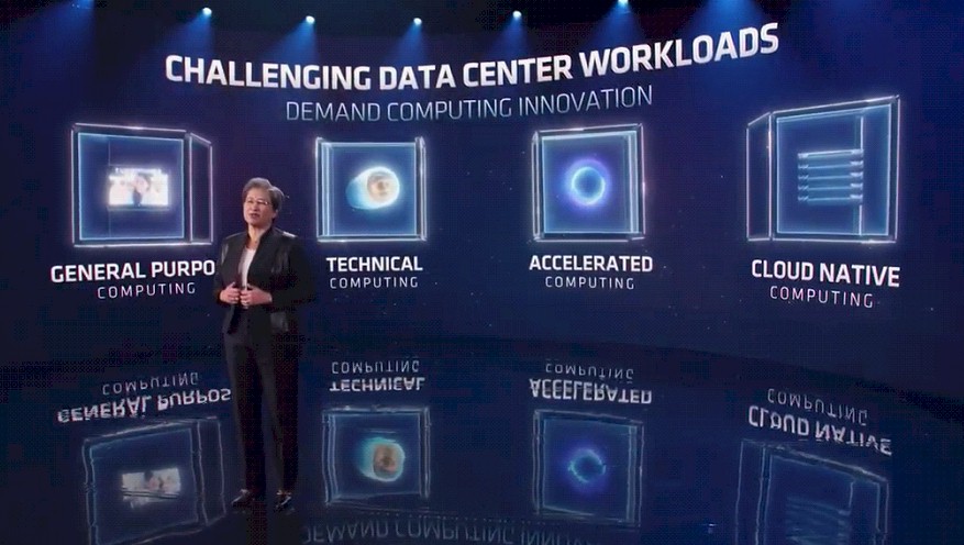
“General purpose computing covers the broadest set of mainstream workloads, both on-prem and in the cloud,” Su explained. “Socket-level performance is an important consideration for these workloads. Technical computing includes some of the most demanding workloads in the datacenter. And here, per-core performance matters the most for these workloads. Accelerated computing is focused on the forefront of human understanding, addressing scientific fields like climate change, materials research, and genomics, and highly parallel and massive computational capability is really the key. And with cloud-native computing, maximum core and thread density are needed to support hyperscale applications. To deliver leadership compute across all these workloads, we must take a tailored approach focused on innovations in hardware, software, and system design.”
With that, let’s take a look at the Epyc roadmap that Su, Norrod, and Papermaster talked about and then look at the augmented and extended one that we put together to give you and even fuller picture.
Here’s the Epyc roadmap they all talked about:
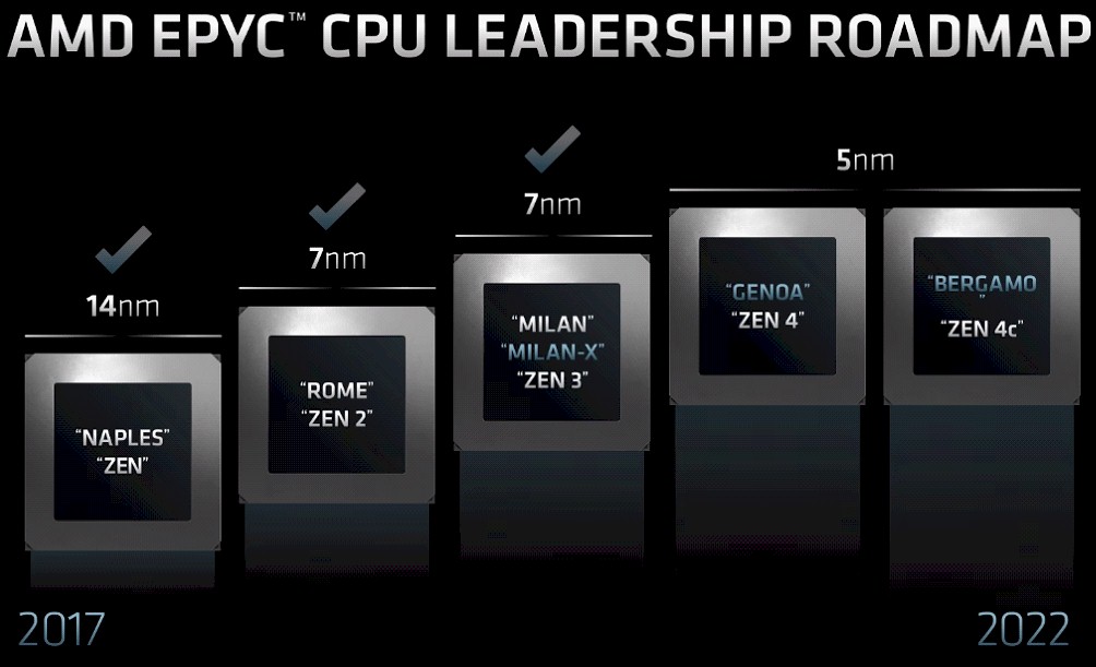
You can see that the “Milan-X” chip has been added, and so has another chip in the “Genoa” series, called “Bergamo” and sporting the Zen 4c core, a variant of the forthcoming Zen 4 core and a different packaging of the compute chiplets than the standard Genoa parts will have. But that’s not all you get.
There is also the “Trento” variant of the Milan processor, which will be used as the CPU host to the MI200 GPU accelerators in the Frontier system. And then there will be a second generation of 5 nanometer Epyc processors, and we have caught wind of a high core count version code-named “Turin,” which now that we see the more revealing AMD server chip roadmap, looks very much like a follow-on to Bergamo, not to Genoa. Which implies a different follow-on to Genoa for which we do not yet have a codename. (Might we suggest Florence? Maybe Venice after that?)
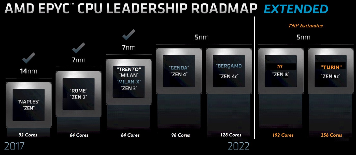
Anyway, here is our extended version of AMD’s Epyc roadmap:
Let’s walk through this.
Milan-X, as we know from this week, will be comprised of a couple of SKUs of the Milan chip with two banks of L3 cache stacked up on top of the native L3 cache on the die, tripling the total L3 cache to boost performance. We know from the presentations that there is a 16-core variant and a 64-core variant, and we presume there might be a few more – variants with 24 cores and 32 cores, possibly 48 cores – with all of them getting the proportional amount of extra L3 cache (3X more per core) added.
With Trento, what we have heard is that the I/O and memory hub chiplet on the Milan processor complex has been enhanced in two ways. The first is that the Infinity Fabric 3.0 interconnect is supported on the I/O hub, which means the Trento chip can share memory coherently with any Instinct MI200 accelerators attached to it. This is a necessary feature for Frontier because Oak Ridge had coherent CPU-GPU memory on the prior “Summit” supercomputer based on IBM Power9 CPUs and Nvidia V100 GPU accelerators. The other enhancement with the Trento I/O and memory hub chiplet is rumored to be support for DDR5 main memory on the controllers. For all we know, the Trento hub chiplet also supports PCI-Express 5.0 controllers and also the CXL accelerator protocol, which might be useful in Frontier.
Milan, Milan-X, and Trento all fit into the SP3 server socket, which tops out at a 400 watt TDP.
With the Genoa and Bergamo chips, AMD is moving to the 5 nanometer chip etching processes from Taiwan Semiconductor Manufacturing Co., and Papermaster said that at the same ISO frequency, this process delivers twice the transistor density and twice the transistor power efficiency while also boosting the switching performance of the transistors by 25 percent. To be super clear: This is not a Milan to Genoa statement, but a 7 nanometer process to 5 nanometer process statement, and how this results in server chip performance depends on architecture and how AMD turns the dials on the frequency and voltage curves. AMD is also moving to a larger SP5 socket for these processors.
Genoa is based on the Zen 4 core, and Bergamo is based on the Zen 4c core that has the same instructions per clock (IPC) improvements over the Zen 3 core in the Milan family of chips – and the same microarchitecture so there are no software tweaks necessary to use it – but it has a different point on the optimization curve for frequency and voltage and has some optimizations in the cache hierarchy that make Bergamo more suited to having more compute chiplets, or CCDs, in the Epyc package. That Zen 4 core IPC uplift is expected to be in the range of 29 percent compared to the Zen 3 core, so this is going to be a big change in single thread performance as well as throughput performance with Genoa. Begamo will take throughput performance to an even higher extreme, but will sacrifice some per-thread performance to get there.
The Genoa Epyc 7004 will have 96 Zen 4 cores across four banks of three compute tiles, for a total of a dozen compute tiles, and an I/O and memory hub that supports DDR5 memory, PCI-Express 5.0 controllers, and the CXL protocol on top of that for linking accelerators, memory, and storage to the compute complex. Genoa is launching sometime in 2022; we don’t have much clarity as to when because AMD is timing itself to keep ahead of Intel, which keeps changing its launch dates for “Sapphire Rapids” and “Granite Rapids” Xeon SPs.
There are a couple of ways to get to the 128 Zen 4c cores that Bergamo will offer. Instead of twelve 8-core compute tiles in the Genoa, the Bergamo chip could employ eight 16-core tiles. The die could also have twelve 12-core tiles, and then dud back some of the cores on each tile to dial the core count all the way back to 128 total cores in the Bergamo package. The latter seems equally likely as the former, but if both processors have twelve memory controllers, as is rumored, then it will be the latter scenario. The Trento I/O and memory hub supports eight compute chiplets and the Genoa I/O and memory hub supports twelve compute chiplets, so AMD could go either way to get to Bergamo, but again, if it used the Trento I/O and memory hub, then Bergamo would be relegated to only eight memory controllers and that would cause a compute to memory capacity and bandwidth imbalance. It looks like Bergamo will use the Genoa I/O and memory hub, therefore, and have some partially dudded cores so it maxes out at 128 cores instead of 144 cores. All Papermaster said is that Bergamo has a different physical design and a different chiplet configuration from Genoa, so everyone is guessing at this point.
The Bergamo chip will plug into the same SP5 socket as Genoa, which is what the hyperscalers and cloud builders care about. Bergamo will be available in the first half of 2023 according to Su, but Norrod initially said that it could be end of 2022 to early 2023 for the launch, and then backed off to say early 2023. It’s not clear why this will take so long to come to market. It could be that the hyperscalers and cloud builders only recently talked AMD into taking the risk and incur the extra cost of making a special SKU of the Gemoa processor.
After that, comes kickers to Genoa and Bergamo, and it is looking like the Bergamo kicker is in fact the rumored 256-core “Turin” processor based on the future Zen 5c core that has been rumored recently.
We don’t think the stock, general purpose kicker to Genoa would jump from 96 cores to 256 cores, but jumping to 192 cores would be reasonable. And so that is what we think will be in the Genoa kicker, which is labeled with “???” in our extended roadmap above. (We will call it Florence until we are told otherwise.) This chip might have four compute tiles, each with twelve Zen 5 cores, in each core complex, and four core complexes on the package to reach that theoretical 192 cores in the general purpose Epyc 7005. The Turin hyperscale variant would have 256 cores and a thermal design point of a whopping 600 watts, so people are saying. The compute tile here could be based on 16 Zen 5c cores, packed into a four-tile compute complex, with four of these on the package.
We think there will be Genoa-X and Florence-X variants with stacked 3D V-Cache, and there is even a possibility to see Bergamo-X and Turin-X variants that also have enhanced L3 caches. Why not?
There is talk that the Epyc 7005s will be based on TSMC’s 3 nanometer processes, but we think AMD will try to get two generations of chips out of 5 nanometers, with the Genoa kicker and Turin based on a refined 5 nanometer process, much as Rome was a first pass at 7 nanometers and Milan is a second pass. This is particularly the case if TSMC is having delays with its 3 nanometer processes, as was rumored two months ago. The Epyc 7005s are probably a late 2024 to early 2025 product – again, it will depend on a lot of moving parts and how well or poorly Intel is doing, and whatever else is happening in the server space at that time. The 10 exaflops generations of supercomputers will require these CPUs.
We strongly suspect that the Genoa kicker and the Turin processor will fit into the same SP5 server socket as Genoa and Bergamo. Server makers freak out if you do a socket change with every generation.

AMD Hits Intel Below The Belt In The Datacenter Wallet
What Intel calls “cloud digestion” as the cause of the massive pullback in spending in its Data Center Group is looking more and more like a case of “Epyc indigestion” for Intel, not for the hyperscalers and cloud builders. And the top brass at Intel should be thanking the heavens …
Ampere Gets Out In Front Of X86 With 192-Core “Siryn” AmpereOne
The largest clouds will always have to buy X86 processors from Intel or AMD so long as the enterprises of the world – and the governments and educational institutions who also consume a fair number of servers – have X86 applications that are not easily ported to Arm or RISC-V …

AMD Finally Breaks The 10 Percent Server Share Barrier
History doesn’t really repeat itself, but it surely does use a lot of synonyms and rhymes, and sometimes, if you listen very closely, you can catch it muttering to itself. It is with this in mind that we contemplate the recent data coming out of Mercury Research, which is the …
My guess is that 4c core is going to cut off avx512 and enable the SoC to squeeze more cores in the same space and power budget. Provided that zen4 with avx512 rumors are true.
@Jure, Zen4’s AVX512 support, if true, could very well be implemented without adding FP execution units, but rather “fusing” the two AVX2 units into a single AVX512 unit. Sure, then you don’t get double the FP throughput but AVX512 has other aspects that accelerate execution even within the same execution resources (more registers, element permutation instructions, etc). I really hope AMD do not introduce feature segmentation there, especially since the article suggests that they will be tuning the F/V curves rather than cutting features. Keeping fingers crossed…
@Jure, @Nikolay: in AMD’s presentation there I slide indicating that Zen 4c has the same ISA, so there will be AVX512.
Zen4c is about reducing Fmax and L3 per core to be able to lower the area.