

Necessity is the mother of invention, and advances in chip packaging are catching up to those in transistor design when it comes to working in three dimensions instead of the much more limited two. And X86 server chip maker AMD is striking first with a new 3D packaging technology for L3 cache on server chips, called 3D V-Cache appropriately enough, that has been married to its current “Milan” Epyc 7003 processors and that is providing a big performance boost for HPC simulation and modeling workloads.
The resulting “Milan-X” processors were previewed at AMD’s Accelerated Computing Premier online event today, which was timed to be a spoiler for Nvidia’s fall GTC 2021 conference, which starts tomorrow. Lisa Su, AMD president and chief executive officer, and her team previewed the Milan-X, which we presume will be a few special SKUs – probably not more than that – of the existing Epyc 7003s when they come out in the first quarter of 2022. Microsoft’s Azure cloud is the first to get its hands on the Milan-X chips, and has released some initial performance specs for the processor, as we report elsewhere on The Next Platform.
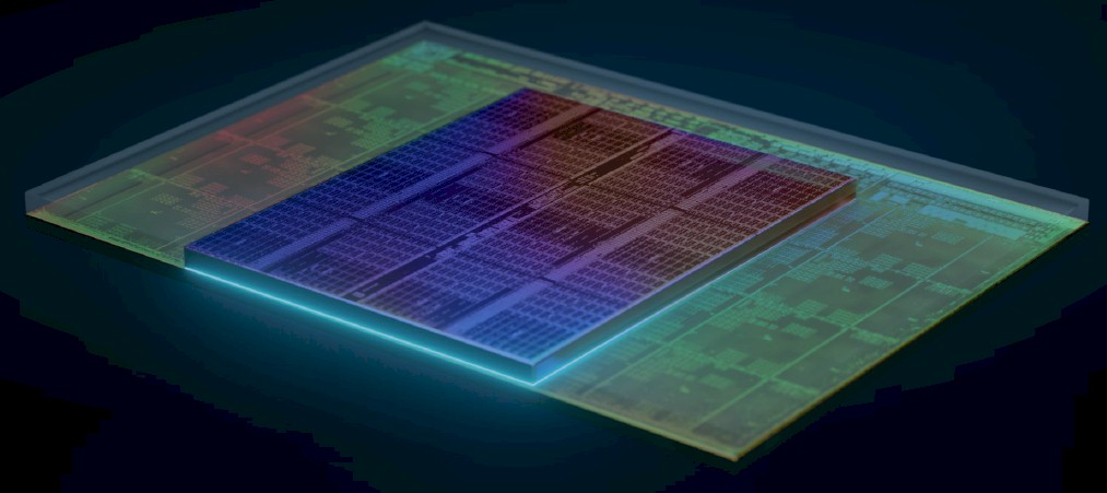
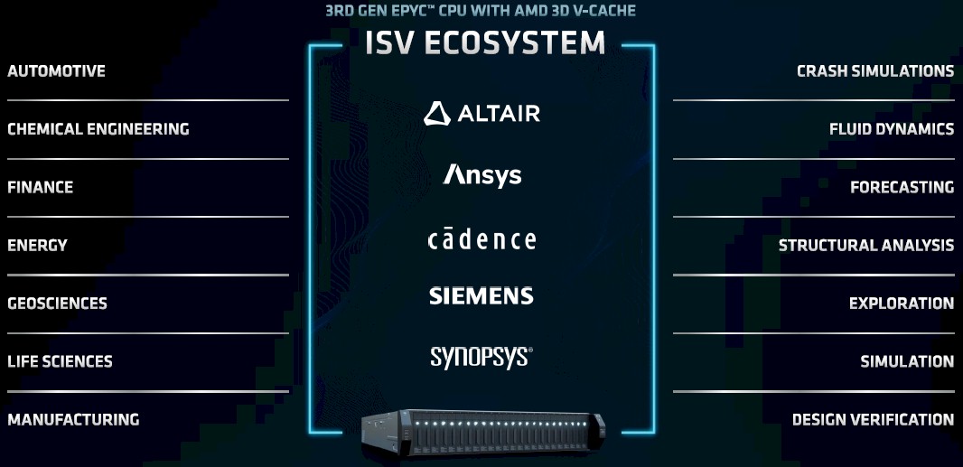
The Milan server processors pack eight chiplets, with eight Zen 3 cores each, and a central I/O and memory hub to create a 64-core socket, much as the “Rome” Epyc 7002 chips did before them. There are lots of innovations between the Rome and Milan generations, which we talked about in our initial coverage of the Milan chips back in March; we drilled down into the Milan architecture further here. The Milan-X has no architectural changes in the processor, and will also top out at 64 cores, but it does have lots of extra L3 cache stacked on top of the compute chiplets in the Milan package. And this extra L3 cache is revving up the HPC applications that it is initially targeted at, which include finite element analysis, structural analysis, computational fluid dynamics, and electronic design automation.
The 3D V-Cache technique was previewed back in June by Su, in this case on a prototype using a Ryzen 5900X processor aimed at desktop PCs. But it has been in development for years by AMD and its foundry partner, Taiwan Semiconductor Manufacturing Co, and moreover, was always intended to be put into production first on server processors.
The Ryzen 5900X processor comes with either 12 or 16 cores in package with two core complex dies, or CCDs as AMD calls its compute chiplets. Each CCD has 32 MB of L3 cache etched onto the chiplet, for a total of 64 MB of integrated L3 cache. With the 3D V-Cache, AMD took another 64 MB of SRAM and stacked it onto of each of the CCDs, and using a direct copper-to-copper interconnect between the SRAM on the compute die and the SRAM stacked on top of it, using through silicon vias (TSVs), and using a process that does not require microbumps or solder to make the links, AMD was able to triple the L3 cache capacity on the Ryzen 5900X prototype to 192 MB.
It is not clear how much this 3D V-Cache approach adds to the cost of a processor, but clearly it is going to be used for specific HPC and AI workloads where cache is king. What AMD did reiterate about this cache stacking technique it co-developed with TSMC was that it had more than 200X the interconnect density of on-package, 2D chiplet packaging techniques and more than 15X the interconnect density of microbump 3D packaging approaches. And perhaps most importantly, it was three times as energy efficient as the microbump 3D approaches.
On the Milan-X, AMD is taking bigger chunks of L3 cache SRAM and plunking it down on top of the L3 cache segments of Milan CCDs. The ratios are the same – 32 MB of L3 cache on the Milan CCDs and 64 MB of 3D V-Cache on top of each CCD in the Milan segment, which works out to a total of 768 MB of L3 cache across the top-bin part of the Milan socket.
“If you add a 512 KB of L2 cache per core, 32 KB each for L1 instruction cache and L1 data cache, there is a total of 804 MB of cache per socket at the top of the stack with Milan-X,” explains Ram Peddibhotla, corporate vice president of product management for datacenter products at AMD. “This is an amazing amount of cache. This additional L3 cache relives memory bandwidth pressure and reduces latency, and that in turn speeds up application performance dramatically.”
It was not made clear, but we suspect that the V-Cache is stacked two high above the native cache. It would be a block copy of the L3 cache, and it would be funny if dud Milan chips had their L3 cache cut out and stacked on top. Why not? Recycle all that you can.
Communicating upwards to L3 cache does have a slight performance penalty compared to accessing the native L3 caches on the CCDs, according to Peddibhotla, something on the order of a 10 percent or so speed reduction in L3 cache accesses. But considering that three times as much data can be stored in L3 cache on the Milan-X chip, that slight delay is dwarfed by the greater access to data and not taking a cache miss that will force a processor to go out to DDR4 main memory, which is around 1,000X slower than accessing L3 cache.
On a wide range of HPC applications that AMD has tested with and without 3D V-Cache, the performance uplift has averaged around 50 percent, which is a big deal. A very big deal. (The Ryzen 5900X prototype only showed a 15 percent performance increase across a bevy of games that were benchmarked. But still, a 15 percent boost in instructions per clock (IPC) represents an architectural generation in processor design these days (more or less), and for the Milan server chips and the HPC workloads, a 50 percent boost is like a leap of three architectural generations.
As an example, AMD showed off benchmarks based on the Synopsis VCS circuit verification tools, which are used to verify chip design as part of an EDA stack. With EDA workloads, simulations of circuits are dispatched to single cores, and the idea is to dispatch many, many different scenarios to thousands or tens of thousands of cores all at the same time. For this work, having a chip with a modest amount of cores helps with compute density and cost, but having a relatively high clock speed also matters because each core is doing its own job.
On the Synopsis VCS test, a 16-core Milan processor without 3D V-Cache was able to complete 24.4 jobs per hour. But with the addition of 3D V-Cache, the same processor was able to handle 40.6 jobs per hour. That is an increase of 66.4 percent in throughout, and chip designers could make use of this extra performance in a number of ways. They could finish their verification earlier and move on to production, or they could run more test scenarios in a given time to create a more robust design. Or, they could split the difference somewhere in the middle.
You may be thinking that an even larger L3 cache could be added to Milan-X, but not so fast. The 3D V-Cache is stacked atop the native L3 cache not only to make TSV connections down into the compute complex, but there would be thermal issues and connectivity issues in putting cache on top of cores. So it might seem like a nice idea if you were thinking of how much L3 cache you might be able to put on the entire CCD – it is probably another 64 MB to 96 MB on each CCD with the 7 nanometer processes used to make the Milan chips. That would be truly amazing, but the magic blue smoke would certainly come out of the Milan-X complex then, and what you have left after that is burnt sand.
But, you can always go vertical, so long as you can get rid of the heat. Just like HBM2 memory is stacked four or eight high, we see no reason, in theory, that L3 cache could not be. The TSVs would have significant latency, of course, the higher that you go. But that extra cache would really boost performance for a lot of workloads. We shall see what AMD does down the road, but eventually, we think that 3D V-Cache and even HBM memory will be standard options for Epyc processors.
Because Milan-X is a real Milan Epyc 7003 processor with the same Zen 3 cores and fitting in the same SP3 server sockets, there is nothing that server builders have to do to adopt Milan-X other than do a BIOS update to let the motherboard know the processor has a much fatter L3 cache.
One last thing: Apparently, the Rome Epyc 7002s had the TSVs that would have allowed it to support 3D V-Cache, and that obviously did not happen. AMD was smart enough not to promise anything it didn’t know for sure it could absolutely deliver on time. As for what SKUs and when it is appearing after the Milan Epyc 7003 launch earlier this year, it is about moving when the technology is ready.
“It was about finding where we thought the sweet spot was, and not just in terms of price/performance,” explains Forrest Norrod, general manager of AMD’s Datacenter and Embedded Solutions Group. “We were introducing a very significant technology that adds a lot of capability down the line. We are doing it in an almost optional way. Milan is a fantastic part, and Milan-X uses 3D V-Cache to make an even more fantastic part. And if 3D V-Cache didn’t work, Milan would still be a fantastic part. We have been working on this a long time, but execution fidelity is paramount and we are not going to do anything to screw up our roadmap. We are always going to look to retire the risk in new technologies in prudent ways, and that was part of the equation as well.”


Is it now possible to place another cache slice or two under the base die? Surely the TSV array doesn’t care whether the connection is on top or bottom. Assuming die thinning is required, this could be the risk factor that rules the idea out.
Typo in the paragraph about Synopsys VCS. You have: “many different scenarios to thousands or tends of thousands” which should be ‘tens’ not ‘tends’.
As a SysAdmin who has supported people running Synopsys VCS jobs, I can see alot of the big compute guys salivating over getting hold of these systems, especially if it lets them make the tradeoff of quicker turn times versus more detailed simulations. Very cool.
“It was not made clear, but we suspect that the V-Cache is stacked two high above the native cache.”
It is only stacked one high. The V-Cache is created on a process that is optimized for cache and is double the density of the normal process that is used for both cache and logic.
Showcasing on ryzen in june and producing now firstly on Epyc: a bit of a tricky plan that should pay (a lot) in the HPC field.
>The Ryzen 5900X processor comes with either 12 or 16 cores in package […]
This is a mistake. The Ryzen 9 5900x processor is only sold with 12 cores. The Ryzen 9 5950x processor is the one with 16 cores.
>It was not made clear, but we suspect that the V-Cache is stacked two high above the native cache. It would be a block copy of the L3 cache, and it would be funny if dud Milan chips had their L3 cache cut out and stacked on top. Why not? Recycle all that you can.
IIRC, AMD addressed this when they introduced V-Cache. They don’t cut the L3 cache from defective Zen3 chips, they manufacture a cache die with optimized cache libraries (the die size of this cache only chip raised eyebrows since it’s denser than the L3 cache on zen3 dies). Also, I don’t think they would stack 2 dies on top of a cpu die since the technology is relatively new and doing so would increase the likelihood of a defect occurring. Adding one stack does so already, adding two would be too risky for a product that’s about to ship. My two cents. Cheers.