
Last week at the Fujitsu Forum in Tokyo, Lisa Spelman, who is general manager of Xeon products and Data Center Marketing at Intel, did a soft announcement of the hybrid Xeon CPU-Arria 10 FPGA hybrid chip that the company has been talking about for years and that is now available to selected customers.
The hybrid CPU-FPGA device is not yet a standard part and the company is not yet releasing all of its feeds and speeds, but eventually we think that Intel will divulge all of the details and let regular organizations outside of a handful of hyperscalers and cloud builders also get their hands on them for innovative uses.
Intel did not initially provide a lot of detail on this special version of the “Skylake” Xeon SP processor, but we did some digging around and Intel gave us a bit more insight than it put out in a blog post that represented the global announcement that this chip was available. We were waiting for some details to try to say something intelligent about the CPU-FPGA mashup, and we are happy to say that we have obtained them. There are still a bunch of unanswered questions, this being a product that is not generally available yet.
It has been four years since Intel first talked about doing a CPU-FPGA mashup, an engineering project that Diane Bryant, the former general manager of the Data Center Group at Intel, divulged was under works back in June 2014. This revelation was made after it had taken on FPGA maker Altera as a foundry customer and a year before it shelled out $16.7 billion to go all the way and acquire Altera to become an FPGA maker and thereby benefit from the use of FPGAs in the datacenter instead of being victimized by them. At the time when the deal was done, Intel chief executive officer Brian Krzanich said that up to a third of “cloud service providers” – what we at The Next Platform call hyperscalers and cloud builders to distinguish between the two types of so-called clouds – could be using hybrid CPU-FPGA systems by 2020. (It was never clear if he really meant a third of customers or a third of servers.) The plan was to create a hybrid CPU-FPGA devices with both the Xeon and the Atom on the CPU side and the lower-end Arria chips on the FPGA side, with the Xeon-Arria chip expected by the end of 2016. As far as we know, there was never a plan to put a Xeon and a higher-end Stratix FPGA in the same package.
This integration of the FPGA with the Xeon CPU has taken a little more time than expected, but Intel did show off a prototype based on a 15 core “Broadwell” Xeon processor and an Arria 10 GX coprocessor at the Open Compute Summit back in March 2016, and the delivery for this was pushed out to sometime in 2017. We guessed at the time that the CPU would be linked to the FPGA using the same QuickPath Interconnect (QPI) high speed links that are used to link multiple processors together in a NUMA shared memory system, and that would interestingly allow for the two devices to share the same DRAM main memory coherently and thereby allow for them to share data without moving them from discrete memories on both devices as is the case when the FPGA is sitting out there on the PCI-Express bus in an adapter card.
Here we are in 2018, and the Arria 10 GX appears to still be the FPGA on the integrated package, but the Xeon portion has been upgraded to a “Skylake” generation. Here is what the chip package looks like:

And here is what the internal block diagram looks like:
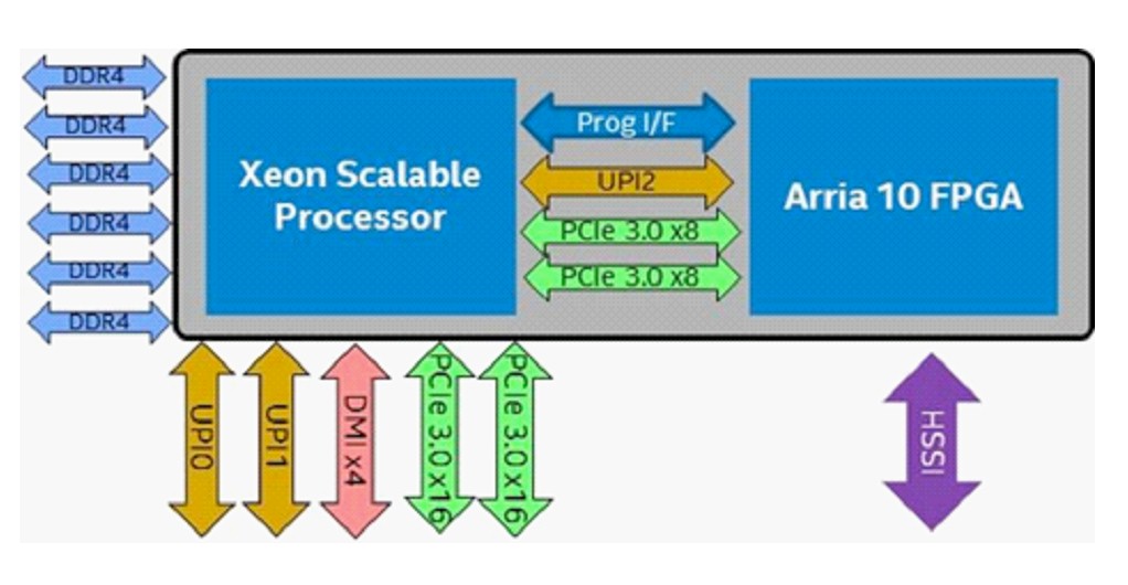
The Skylake Xeon SP processor used in the CPU-FPGA hybrid has three UltraPath Interconnect (UPI) coherent links on it, with this being a follow-on to QPI that, interestingly, has 20 lanes of traffic even though it is a kicker. UPI, at 10.4 GT/sec, is just a faster QPI, which topped out at 9.6 GT/sec, with some other goodies thrown in and not really a huge architectural change. This is about marketing mostly, we think, and preparing the way for other devices to be linked into the Xeon compute complex. In any event, the QPI and UPI links are broken into quadrants, and these quads can be used independently to route traffic between processors.
With two QPI or UPI links, two processors can be tightly coupled to each other and share main memory, looking for all intents and purposes as a single processor with a single memory space as far as the operating system and its applications are concerned. With the Xeon E5-4600 processors and certain Skylake processors, Intel puts three QPI or UPI ports on the chip, allowing for up to four processors to be coupled together in a NUMA system. With this hybrid CPU-FPGA chip, the Xeon SP has three UPI channels, and two of them are used to make a two-socket system and the other is used to link the CPU to the FPGA. This block diagram is, therefore, only half of the system, since two Xeons can be linked to each other, each with one Arria 10 GX FPGA attached. Each Xeon has six DDR4 memory controllers, like a regular Xeon SP, and has two PCI-Express 3.0 x16 slots and one DMI x4 slot hanging off it for other peripherals. Interestingly, two of the PCI-Express 3.0 x8 slots are used to provide additional peripheral connectivity into the Arria 10 GX FPGA, and there is yet another unexplained programming interface between the two devices. There is also a high speed serial interface (HSSI) directly into the FPGA, but we have heard that the direct interface is actually implemented as a 100 Gb/sec Ethernet link.
One of the things that everyone will want to know is what the latency is between the FPGA and the memory sitting on the Xeon processor. All that we can tell you is that the latency is lower than going over the PCI-Express bus with a peripheral card variant of the Arria 10 GX – yes, Intel was stating the obvious and also obfuscating in that response – but it will no doubt be higher than a Xeon talking to the memory on its own DDR4 controllers. It stands to reason that it can’t be worse than one Xeon access the memory of the other Xeon in a two-way NUMA pair, but there may be additional overhead as the memory controller on the Arria 10 GX FPGA talks to remote memory and has to pass through a CPU to get to it.
The Skylake portion of the CPU-FPGA hybrid is called the Xeon SP-6138P, and presumably that means it is a special version of the regular Xeon SP-6138 Gold that supports faster memory and larger memory like the other Platinum chips in the Skylake lineup. The Platinum 81XX and Gold 61XX chips all have three UPI links activated; the Gold 51XX chips only have two UPI links, so you can’t have an FPGA on the same package if you also want to have two-socket server. (If Intel had eight memory controllers on the Skylake die, it might have only done a single socket FPGA hybrid.) This Xeon SP-6138P in the hybrid CPU-FPGA has a thermal design point of 125 watts and this suggests that it is a 20 core chip like the regular Xeon SP-6138P, but that the processor cores have been geared down to around 2.0 GHz to shave 25 watts off the TDP. (The regular Xeon SP-6138G is rated at 150 watts at 2.4 GHz across 20 cores.) The FPGA is rated at 70 watts, and it is a full-blown Arria 10 GX 1150. This FPGA has its own cache memory and does not include ARM cores as etched next to the FPGA gates like some Arria and Stratix chips from the Altera line do.
The initial workload that Intel is targeting is putting Open Virtual Switch, the open source virtual switch, on the FPGA, offloading some switching functions in a network from the CPU where such virtual switch software might reside either inside a server virtualization hypervisor or outside of it but alongside virtual machines and containers. This obviates the need for certain Ethernet switches in the kind of Clos networks used by hyperscalers, cloud builders, telcos, and other service providers and also frees up compute capacity on the CPUs that might otherwise be managing virtual switching. Intel says that by implementing Open Virtual Switch on the FPGA, it can cut the latency on the virtual switch in half, boost the throughput by 3.2X, and crank up the number of VMs hosted on a machine by 2X compared to just running Open Virtual Switch on the Xeon portion of this hybrid chip. That makes a pretty good case for having the FPGA right close to the CPU – provided this chip doesn’t cost too much.
We have no idea what Intel is charging for this. A Xeon SP-6138G chip running at 2 GHz across those 20 cores has a list price of $2,612 each when bought in lots of a thousand from Intel. This is at the high end of midrange in terms of pricing for the Skylake line, nothing too crazy. Pricing on the Altera FPGAs is almost a state secret, and frankly, FPGAs are a lot more expensive than most people want to talk about. We have seen Arria 10 GX 1150 development kits costing between $4,200 and $10,000, and we could argue that the integration should be cheaper since the FPGA won’t have its own memory or card. This is kinda the point of integrating it in the socket, which is to lower the cost and improve the programmability of the hybrid device and thereby drive adoption and increase the market. Given this, we think it should probably have a list price in the range of $6,500 – the low-end of the range of the FPGA plus the cost of the CPU. That is a lot better than trying to buy top-end Xeon SP-8180M parts (which cost $13,011 a piece at list price) to try to do more Open Virtual Switch work on the server natively on the CPU and still have lots of computer left over for the VMs. Half of the cores will be used to run Open Virtual Switch, as Intel just showed. Intel says this will be a limited part for now and will not have a list price for now, but that it will eventually get one as it ramps.
There are all kinds of possibilities for this hybrid CPU-GPU device. It can be an inference engine for machine learning, as well as other kinds of network offload and data preprocessing and manipulation that is done on CPUs or even FPGA-enabled network cards these days. In a sense, the FPGA is just getting moved down a bump in the wire and to the CPU where Intel can make better programming. Intel will get the FPGA sale either way, whether it is implemented on a PCI card or within a CPU socket. But this way, it can sell against Xilinx in a fashion that the latter vendor cannot easily counteract. Unless it does in-package hybrid compute deals with AMD, IBM, Cavium, and Ampere. Which could very well happen.
Fujitsu plans to have this Xeon-Arria hybrid chip integrated into its Primergy server line by the fourth quarter; it is not clear when others will get access, but you can bet the hyperscalers and cloud builders already have it if they want it.

AMD Finally Reaps The Fortunes It Has Sown
Sometimes, competing for business means coming up with better products than your rivals. And other times, competing means just not screwing up while your competitor stumbles. For the heated battle between AMD and its archrival, Intel, when it comes to compute engines in the datacenter, AMD is in the fortunate …
Intel Chip Research Pushes Power Efficiency And Performance
Since Pat Gelsinger’s return to Intel as chief executive officer in early 2021, the company has bet big on bolstering its manufacturing processes and foundry business, expanded its fab footprint in the United States, and advocated for expanding the country’s chip making capabilities. Intel’s success – or failure – in …

Intel’s “Ponte Vecchio” GPU Better Not Be A Bridge Too Far
It is pretty obvious to everyone who watches the IT market that Intel needs an architectural win that leads to a product win in datacenter compute. And it is pretty clear that the top brass at Intel are putting a lot of chips down on the felt table that the …
@Tim — Can you pls comment on GPU/NVLink latency vs Xeon/FPGA latency. Also how can solns be deployed with multiple FPGAs — similar to multiple GPUs in a box?
@Tim — https://pmem.io/ — How (to use/ will this fit-in) in a GPU/FPGA soln
I’d like to know if anybody has verified that the HSSI connection is actually present on the 6138p package as shown in the block diagram. I sure hope it is, but the publicity photo above shows an LGA 3647 package *without* HSSI. Instead of using a NIC, I want to be able to plug a 6138P directly into a network with a bracket and cable like this: https://www.mouser.com/new/TE-Connectivity/te-connectivity-chipconnect-cable-assemblies/
Who wants the thing. Now we know the security processor in all of these is compromised from the start. How many machines of all types right now are completely wide open? More firmware fixes? Why not do another 10% increase in mips and sell another generation.
What is “the security processor?”
AKA management processor or service processor. Small processor added that supports over-network computer management. Used to configure BIOS, drives, install OS etc remotely. Very useful when you have remote machines. But it has full access to the main processor and platform so you’d want access to it tightly controlled. Sadly on Intel the security for XEON service processors has been broken. None of this has anything in particular to do with these XEON/FPGA products, though their service processors are probably vulnerable also.
These kinds of integrations have been tried in the past — usually as a coprocessor in another CPU socket. The problem is the hybrid chip doesn’t fit into the the main processor future roadmap and gets obsoleted as soon as the next generation of Xeons comes out. The FPGA fabric is also 4x slower than the CPUs and can’t keep up with the UPI data rates.
Unless Intel can guarantee a future roadmap for these chips, very few customers will spend the time to develop on the FPGA (whose development times are 10x slower than writing software). Those who tried it on previous generations have moved back to non-hybrid solutions (e.g. Exegy).