

At long last, Intel’s “Skylake” converged Xeon server processors are entering the field, and the competition with AMD’s “Naples” Epyc X86 alternatives can begin and the ARM server chips from Applied Micro, Cavium, and Qualcomm and the Power9 chip from IBM know exactly what they are aiming at.
It is a good time to be negotiating with a chip maker for compute power.
The Skylake chips, which are formally known as the Xeon Scalable Processor family, are the result of the convergence of the workhorse Xeon E5 family of chips for two-socket and four-socket servers with the higher-end Xeon E7 family of processors that were designed for machines with four or eight sockets using Intel’s on-chip NUMA clustering or even larger machines with Superdome and NUMALink chipsets from Hewlett Packard Enterprise. By converging the Xeon E5 and Xeon E7 into a single line, which we discussed back in May when Intel unveiled some high-level information about its plans, Intel can span a great range of performance with a single chip family and simplify the engineering work done by system makers, who had to create radically different designs for the former Xeon E5 and Xeon E7.
That is not to say that the Xeon Scalable Processor family is not complex; it most certainly is. Intel has a lot of bells and whistles on the three variants of the Skylake processor, and it turns a lot of knobs and buttons to activate and deactivate features and to provide technical differentiation across the line and different price points based on the number of cores, clock speed, maximum main memory, NUMA interconnect bandwidth and port count, L3 cache sizes, thermal footprint, and price. Picking out the right processor for the job is not that much easier, although now, with a single Socket P to plug into, at least systems are, in theory, more malleable than when the Xeon E5 and Xeon E7 were very distinct in terms of socket form factor and the type of DDR4 main memory used. (The Xeon E7 chips used buffered memory cards, while the Xeon E5s did not.)
The Skylake Xeons are coming to market pretty much as we anticipated back in May 2015, when the Skylake and related “Purley” server platform roadmap was accidentally leaked by an Intel employee in Europe. The top bin part does indeed have 28 cores, as expected, and there is a new, faster link called UltraPath Interconnect that replaces the QuickPath Interconnect that made its debut back in March 2009 with the transformational “Nehalem” Xeon 5500s that took a lot of the ideas from AMD’s Opterons and drove AMD from the datacenter. The Purley platform is only missing one of the key ingredients that was one the roadmap: the “Apache Pass” Optane persistent memory based on the 3D XPoint created by Intel and Micron Technology. This is being ramped now and will come to market early next year, so we hear.
There is a lot in the Skylake launch, and with this being what amounts to two big server launches and one little one (the four-socket Xeon E5 never got top billing) all rolled into one, we are going to take our time and drill into all the aspects of the new chips and the new way in which Intel is assembling its platform as it faces the toughest competition it has seen since rising to the top of the datacenter. We are starting with the basic feeds and speeds in this story and then will go into the architecture of the Purley platform and the microarchitecture improvements in the Skylake chip, memory and I/O subsystems, performance on various workloads, special features aimed at HPC, deep learning, and enterprise workloads, price/performance analysis versus prior Xeon E5 and Xeon E7 chips, and comparisons with AMD’s new Epyc lineup – the latter being the most obvious and easiest chip to pit against the new Skylakes because of its X86 compatibility.
What Is In A Name?
The Skylake Xeons represent as big of a change in marketing and sales as they do a leap in technology for Intel. The name Scalable Processor is intended to convey that there is a single line, and Xeon SP is as convenient as Xeon E5 and Xeon E7, so people will get used to it. It is important to note that the Xeon SP family does not scale down to a single socket formally, although there is no reason why a server maker could not create a single-socket implementation of a Xeon SP. Intel seems content to push its Skylake Xeon E3 and Broadwell Xeon D processors down into this space, where microserver and storage workloads dominate. But, to be truly scalable, there should have been a bunch of Xeon SP SKUs tailored to the single socket crowd – especially given the fact that AMD is pushing single socket Epyc 7000 series machines aggressively against mainstream two-socket Xeon systems and making a compelling argument that its single socket machines have enough compute, memory, and I/O capacity and memory and I/O bandwidth to take on the midrange of the Xeon line and win in terms of performance and price/performance. Intel will need to counter here with its own single socket story, and we expect that it will. But not today.
As Intel previously disclosed, there are four different classes of Xeon SP chips, and they are given Olympic medal names – Bronze, Silver, and Gold – plus the ultimate Platinum designation for the SKUs for the chips with the highest number of features and the highest capacities activated. At the last minute, Intel had to add in an extra level of Gold, and it has left space somewhere between Gold and Platinum for the Xeon Phi or other hybrid Xeon chips with Altera FPGAs or Nervana neuromorphic processors to slide in. Here is the secret decoder ring that explains the new Xeon SP naming conventions:
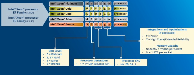
You will note that there is no Copper, Aluminum, Steel, Iron, Stone, or Wood levels of processor, but there is room in the naming conventions for two more levels below Bronze and three if you don’t mind starting with zero instead of an integer. There is room above as well, but only one more to nine unless you want to add a digit to the name.
The Platinum processors have everything turned up high and offer the most scalability variance with support for machines with two, four, or eight sockets without resorting to external chipsets. The Platinum 81XX chips have the highest frequency at 3.6 GHz for a four-core variant and have the most I/O with all six memory DDR4 channels and all 48 lanes of PCI-Express 3.0 activated; they also have all three UPI paths turned on and running at the top speed of 10.4 GT/sec, and sport the fastest DDR4 memory available on Purley systems, running at 2.67 GHz. The full AVX-512 vector math unit is also turned on in the Platinum machines, and in the models with the M designation the main memory stretches to 1.5 TB per socket instead of the 768 GB per socket maximum on the other models. Turbo Boost overclocking and Hyper-Threading simultaneous multithreading of two threads per core are also all activated on the Platinum variants of the Skylakes. These are roughly analogous to the Xeon E7-8800s.
The Gold variants of the Skylake Xeons come in two flavors: the 61XX and 51XX series. The higher end Gold 61XX series supports up to 22 cores and support two or four socket machines and have up to three UPI links per socket running at the 10.4 GT/sec rate. If you had to make an analogy, these are like the Xeon E7-4800s. The 61XX series can run memory at the 2.67 GHz top speed and have a variant with six cores that can hit 3.4 GHz, and have full AVX-512 support with two fused multiply add (FMA) units running like the Platinum 81XX series.
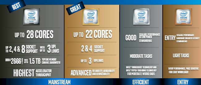
With the Gold 51XX series, which aligns somewhat to the Xeon E5-4600s of the past, the core count is stepped down to a maximum of 14 cores, only two UPI links are available (running at the full 10.4 GT/sec speed), main memory tops out at 2.4 GHz, and the AVX-512 unit has only one FMA unit turned on. The Gold 51XX series can be used in machines with two or four sockets, but like the Xeon E5-4600, moving them to four sockets increases latencies because the system has to be hooked together in a ring and sometimes there are two hops to access remote memory chunks instead of one hop.
The Silver 41XX series replace the middle of the road Xeon E5 chips, the ones commonly used by enterprises that do not need to cram as many cores as possible into a system and that are looking for the best price/performance. The Xeon SP 41XX chips scale up to a maximum of 12 cores, and a 10 core version has the top speed of this series at 2.2 GHz, which is not all that fast, mind you. But companies buying in the belly of the market don’t buy chips with a lot of cores or with higher clock speeds. We could make a credible argument that companies should do this, and to tune their iron to their workloads, like a hyperscaler or HPC center would. And we think that the Xeon SP line was created precisely so Intel and its server partners could start doing this in earnest without having to negotiate the Xeon E3-Xeon E5-Xeon E7 barriers. In any event, the Silver 41XX series has up to 768 GB of memory per socket, has two UPI links to create two-socket NUMA systems, although they run at a slower 9.6 GT/sec rate. The AVX-512 unit has only one FMA unit activated, just like the Gold 51XX series. Turbo Boost and HyperThreading are turned on.
That leaves the Bronze 31XX series, which we do not expect to get a lot of play in the datacenter. These chips top out at eight cores and at a 1.7 GHz clock speed, which is not all that great. They do have the full 48 lanes of PCI-Express bandwidth available, which could make them interesting for network function virtualization and storage workloads where a single socket Xeon E3 might be chosen, but the main memory only runs at 2.13 GHz. The Bronze 31XX series of chips have two UPI links running at the slower 9.6 GT/sec and can support two-socket NUMA setups; the AVX-512 vector unit has only one FMA activated, as with the other lower end Xeon SP chips.
There Can Only Be Three
As has been the case with past Xeon E5 processors, there is not actually one version of the chip, but multiple ones. With the Broadwell chips, there were actually six variants: one Xeon E3, one Xeon D, three Xeon E5s, and one Xeon E7. By converging the Xeon E5 and Xeon E7, Intel is able to eliminate one chip variant, converge to a single socket, and also reduce the SKU count and, frankly, some confusion over which chip to buy when.
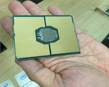
By the way, Intel is no longer providing die shots of the Xeon chips, but we found the Skylake lurking in a presentation a few months back, and here it is:

Intel has made a lot of changes with the Skylake design, which we will got into in further detail in a subsequent story, but we will summarize them here. Not only did the Skylake core get AVX-512 support akin to that in the “Knights Landing” Xeon Phi 7000 series many-core parallel processors, but Intel has radically changed the interconnect on the chip that glues the cores and other components together, shifting to a mesh interconnect that borrows some ideas from Knights Landing from a ring structure that was getting very hairy indeed with the Broadwell and Haswell Xeons of prior generations.
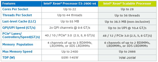
Intel has also radically changed the cache structure of the Skylake processors, boosting the L2 cache from 256 KB to 1 MB per core which also shifting to a smaller, non-inclusive distributed shared L3 cache that can shrink thanks to tweaks and the larger L2 cache and also leave more room for more cores on the die. The number of memory channels on the Xeon SP is six, up from four with the Broadwell and Haswell Xeon E5s, but there are only two memory sticks per channel so the maximum number of DIMMs per system remains the same, which is why the memory capacity is also the same. For performance reasons, a lot of customers using prior Xeon E5 chips only put two DIMMs on a channel, so this will look like a 50 percent increase in memory capacity and an even larger increase in memory bandwidth to them because the memory is also running faster in a lot of cases. Each Skylake socket supports a dozen PCI-Express controllers for 48 lanes of traffic, which is a modest 20 percent boost in I/O per socket. As expected, there are variants of the Skylake Xeons that have the 100 Gb/sec Omni-Path interconnect on the package.
There is not, by the way, a correlation between the metal level of a Skylake processor series – Platinum, Gold, Silver, or Bronze – and its die type – Extreme Core Count, High Core Count, or Low Core Count, which are known as XCC, HCC, and LCC in the Intel lingo. With the Skylakes, there is no Mid Core Count or MCC variant, which might have had 14 cores. The idea was to eliminate one unnecessary die type with the Xeon E5-Xeon E7 convergence.
Here is what the XCC variant looks like:
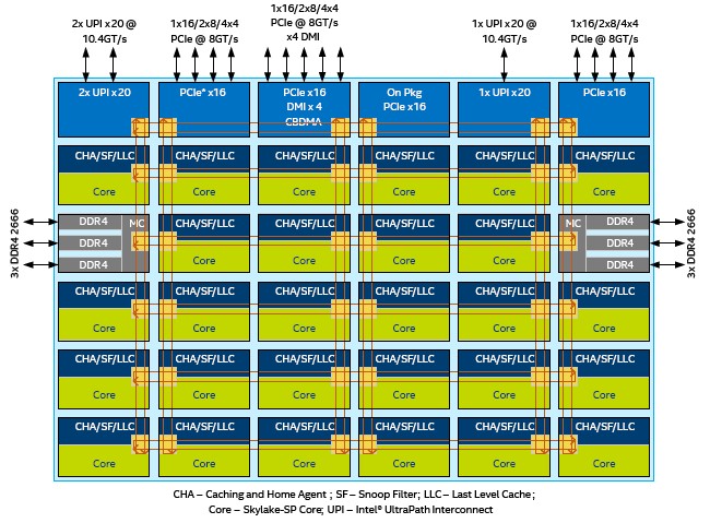
There are five rows of cores and L3 caches, as you can see, and these elements are linked to each other and to the I/O controllers at the top of the die and the two sets of three DDR4 controllers on the sides of the die by a 6×6 mesh interconnect. This chip has 28 cores on the die, and any chip with three UPI links is using the XCC die.
Take a gander at the HCC and LCC dies:
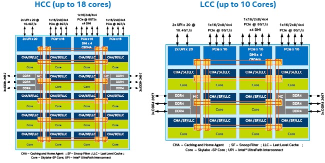
These two Skylake Xeon variants have only two UPI links, and they differ from each other primarily in terms of the number of cores handing off the mesh. The HCC chip has five rows of cores, but is only four cores wide, and hits 18 cores after the memory controllers take out two of the cores that might have been there. The LCC chip cuts it back to three rows of four cores, and has the same two memory controllers. It is interesting that Intel has not put out a Xeon SP that has only one set of memory controllers activated, and we think that a future 21XX and 11XX series at the low end, perhaps for single socket machines, will do this. But that is just a guess.
The Feeds And Speeds
With these three dies and the twisting of many knobs and the pulling of many levers on the Skylake architecture, Intel is bringing out 51 variants of the Xeon SP chips, which is a much lower SKU count than the Xeon E5 and Xeon E7 of the Broadwell generation from last year added together. (We suspect that there are dozens of additional custom parts being made for hyperscalers and cloud builders.)
There are four different groupings of the Skylake Xeons, which are outlined below with their basic feeds and speeds and pricing for 1,000-unit trays.
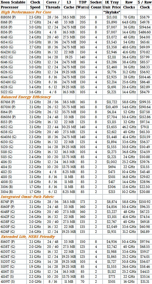
The four groupings are as follows. The first group is for chips that have the highest per-core performance and incidentally, that are only available for machines with four or eight sockets. (Although we suspect that companies could decide to use these in two socket systems if they wanted to, but it would be very pricey indeed. But a hyperscaler getting 50 percent off and designing its own systems can do this.) Some of these chips bust above 200 watts in thermal draw, which is IBM Power-class juicy drinking and heat dissipation. (And that, dear friends, is not a coincidence.)
The second grouping is balanced for energy efficiency and performance per watt, and spans machines that have two, four, or eight sockets. Together, these account for 35 of the 51 Skylake Xeon SKUs. There are another seven Skylake Xeons that have lower clock speeds and therefore lower thermals as well as integrated Omni-Path Interconnect ports on the package, which are clearly aimed at the HPC and AI crowds. The final nine machines in the Skylake lineup have hardened packaging that makes them suitable for NEBS-compliant, long-term use in the field in telco and other kinds of gear.
In the table above, we have done a rough calculation of relative price/performance across the Skylake line by multiplying the cores by the clock speeds and dividing this into the list price, but we have a much more sophisticated analysis coming. So stay tuned.

Intel’s Datacenter Decline Not As Bad As Expected
Incoming chief executive officer and long-time Intel employee Pat Gelsinger is talking the helm of a chip company that has plenty of issues to sort out, but there is some good news as Intel reports its financial results for the fourth quarter of 2020 and Gelsinger gets ready to take …
Nvidia, AMD, And Intel Help Stuff The Coffers At Ayar Labs
Everybody wants to get rich in AI these days, and if you can’t do it by investing in the compute engine makers or the hyperscalers and cloud builders, then the next best thing to put your money into is probably some form of optical I/O. It is no secret that …
Intel Fields A 10 Nanometer Server Chip That Competes
At long last, Intel is finally shipping a Xeon SP processor that is based on a 10 nanometer chip manufacturing process and it is finally able to do a better job competing on the technical and economic merits of its Xeon SP processors as architected rather than playing the total …
I was expecting this release to be a lot more impressive than it is. AMD Epyc has eight channel memory, up to 2TB per socket, 128 PCI-e lanes, 32 cores for a fraction of the price of the highest end Skylake-SP. Skylake doesn’t seem to have anything to compete with AMDs fully encrypted memory either.
The only cases i can see choosing these over Epyc would be if you need AVX-512(ARM can do better) or if you absolutely needed 4-8 sockets gluelessly. SPARC would probably be better for scale up in that case though. Intel still has 46bit physical addressing but ARM and Epyc are 48bit for bigger NUMA setups anyway.
Those AVX-512 units must burn a lot of power to hit 205W too.
5118 (G) is 12 core to 16 core
Intel’s infamous product segmentation has once again made itself apparent, while AMD appears to offer more of the vary same PCIe features, Extra memory channels, and other features across all of its Epyc line of server/workstation/HPC SKUs. Also, a little while back, AMD did some seismic workloads/other benchmarks and AMD did mention that there will be a more Direct Attached GPU accelerator capability, via the Infinity Fabric, for Epyc CPUs to coherently interface with any Vega based GPU Micro-Architecture FP/AI SKUs for a similar to NVLink type of inter CPU to GPU(and GPU to GPU/other Infinity Fabric enabled) processor communication on AMD’s latest Epyc platform. How this is implemented, I hope, will be discussed in greater detail at this year’s SIGGRAPH.
AnandTech(1) has had access to Epyc(One Week) and to Intel’s SkyLake(Two Weeks) Xeon Scalable Processor SKUs. So They have had some time to test a few things out and compare Epyc to SkyLake SP(Xeon). It’s a good Read of 23 sections with various introductions to both the Intel and AMD competing platforms and some useful benchmarks and power testing etc.
“First of all, we have to emphasize that we were only able to spend about a week on the AMD server, and about two weeks on the Intel system. With the complexity of both server hardware and especially server software, that is very little time. There is still a lot to test and tune, but the general picture is clear (1).” [See Closing Thoughts page]
(1)
“Sizing Up Servers: Intel’s Skylake-SP Xeon versus AMD’s EPYC 7000 – The Server CPU Battle of the Decade?”
http://www.anandtech.com/show/11544/intel-skylake-ep-vs-amd-epyc-7000-cpu-battle-of-the-decade
Or quickly summarized there is no clear winner, it all depends on what your workload is and your needs
When you consider the price difference though, AMD does have an advantage. Perhaps in power efficiency as well in many applications thanks to Zeppelin.
There is remarkably little progress, to say it mildly, in the CPUs $/raw-clocks number. While constructing a cluster a few years ago, I used i7-5820K, 6c., and overclocked them from nominal 3.4 to ~4.0 GHz. This is 19.6 $/clocks, or 16.7 $/clocks after O/C, price was about $400. The current table of dozens and dozens of Intel CPUs does not even have one processor below
20 $/sum-of-GHz!